Delivering more actionable and strategically valuable research, The Business Research Company’s 2026 market reports feature market attractiveness analysis, total addressable market evaluation, company benchmarking matrices, interactive Excel dashboards, expanded supply chain intelligence, emerging startup coverage, and detailed product insights.
Wafer Fab Equipment Market Forecast: What Market Value Is Expected By 2030?
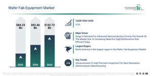
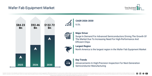
The wafer fab equipment market size has shown substantial growth in recent years. It is anticipated to expand from $84.23 billion in 2025 to $92.46 billion in 2026, achieving a compound annual growth rate (CAGR) of 9.8%. The growth observed in the historic period is primarily due to increasing demand for semiconductor devices, the rise of mobile and consumer electronics, expansion of fab capacities in asia, technological advancements in lithography, and the globalization of semiconductor supply chains.
The wafer fab equipment market size is anticipated to exhibit robust growth in the coming years, with projections indicating an expansion to $132.72 billion by 2030, registering a compound annual growth rate (CAGR) of 9.5%. This growth during the forecast period is attributable to several factors, including the expansion of AI and autonomous systems, the uptake of 3nm and smaller nodes, a rising demand for energy-efficient semiconductor manufacturing, the proliferation of foundries in emerging regions, and the development of next-generation memory and logic devices. Key trends for this period encompass advanced process control systems, miniaturization coupled with high-density fabrication, the integration of multi-functional equipment, high precision wafer patterning, and the adoption of adaptive maintenance and predictive diagnostics.
Download A Free Sample Report For Comprehensive Market Insights:
#Wafer Fab Equipment Market Growth Factors: Which Forces Are Supporting Market Expansion?
Increased demand for sophisticated semiconductors is anticipated to fuel expansion in the wafer fab equipment market. These advanced semiconductors are specialized electronic components built for intricate functions, offering high speed, efficiency, and reliability, finding applications in innovative fields like artificial intelligence, 5G communications, high-performance computing, and future consumer electronics. The escalating demand stems from the requirement for quicker, more efficient processing within contemporary devices, leading to enhanced performance and better energy usage. Wafer fab equipment facilitates the manufacturing of advanced semiconductors by supplying the exact tools and machinery necessary for producing high-performance chips accurately. As an illustration, the Semiconductor Industry Association (SIA) forecasts that global semiconductor industry revenue will climb from $588.4 billion in 2024 to $654.7 billion in 2025, signifying the escalating need for advanced chips. Consequently, the expanding need for advanced semiconductors is propelling the development of the wafer fab equipment market.
Wafer Fab Equipment Market Segmentation: How Is The Market Structured Across Key Categories?
The wafer fab equipment market covered in this report is segmented –
1) By Equipment Type: Photolithography Equipment, Epitaxy Equipment, Etching Equipment, Deposition Equipment, Ion Implantation Equipment, Chemical Mechanical Planarization (CMP) Equipment, Testing Equipment, Metrology Equipment
2) By Fabrication Process: Front-End-Of-Line Processing, Back-End-Of-Line Processing
3) By Functionality: Production Equipment, Research And Development Equipment, Maintenance Equipment, Quality Control Equipment
4) By Application Sector: Integrated Circuits (ICs), Micro-Electro-Mechanical Systems (MEMS), Light Emitting Diodes (LED), Power Devices, Radio Frequency (RF) Devices, Optoelectronics
5) By End-User: Semiconductor Manufacturers, Foundries, Fabless Companies, Research Institutions, Academic Institutions
Subsegments:
1) By Photolithography Equipment: Stepper, Scanner, Mask Aligner, Track System
2) By Epitaxy Equipment: Chemical Vapor Deposition (CVD) Epitaxy, Molecular Beam Epitaxy (MBE), Metal-Organic Chemical Vapor Deposition (MOCVD), Atomic Layer Deposition (ALD)
3) By Etching Equipment: Wet Etching Equipment, Dry Etching Equipment, Plasma Etching Equipment, Reactive Ion Etching (RIE) Equipment
4) By Deposition Equipment: Physical Vapor Deposition (PVD) Equipment, Chemical Vapor Deposition (CVD) Equipment, Atomic Layer Deposition (ALD) Equipment, Electrochemical Deposition (ECD) Equipment
5) By Ion Implantation Equipment: High-Energy Ion Implanter, Medium-Energy Ion Implanter, Low-Energy Ion Implanter, Plasma Immersion Ion Implantation (PIII) Equipment
6) By Chemical Mechanical Planarization (CMP) Equipment: Single-Station Chemical Mechanical Planarization (CMP) Equipment, Multi-Station Chemical Mechanical Planarization (CMP) Equipment, Hybrid Chemical Mechanical Planarization (CMP) Equipment, Polishing Pads And Slurries
7) By Testing Equipment: Wafer Testers, Probe Stations, Electrical Test Equipment, Functional Test Equipment
8) By Metrology Equipment: Critical Dimension (CD) Metrology Equipment, Overlay Metrology Equipment, Thin Film Measurement Equipment, Defect Inspection And Review Equipment
Wafer Fab Equipment Market Innovation Trends: Which Developments Are Transforming The Industry?
Leading companies in the wafer fab equipment market are concentrating on developing sophisticated products, such as high-sensitivity inspection systems, to ensure superior quality and reliability in semiconductor manufacturing. These high-sensitivity inspection systems are advanced tools used in semiconductor fabrication to identify minute flaws or irregularities on wafers and chips, thereby enhancing product quality, boosting output, and reducing the likelihood of device failures. For instance, in December 2023, Hitachi High-Tech Corporation, a Japan-based manufacturer of cutting-edge technologies and instruments, introduced the GT2000 high-precision electron beam metrology system. This system draws on Hitachi High-Tech’s expertise in CD-SEM technology and is specifically designed to address the challenging demands of semiconductor device development and mass production in the High-NA EUV generation. It incorporates a 100V ultra-low acceleration voltage and ultra-high-speed multi-point measurement capability that minimizes resist damage, enabling accurate and rapid inspection of advanced 3D semiconductor devices, including those with GAA and CFET structures. The aim of this system is to enhance both yield and measurement accuracy within advanced semiconductor manufacturing processes, supporting both research and development as well as mass production stages.
Wafer Fab Equipment Market Competitive Landscape And Leading Companies
Major companies operating in the wafer fab equipment market are Hitachi Ltd., ASML Holding N.V., Canon Inc., Applied Materials Inc., Komatsu Ltd., Texas Instruments Incorporated, Lam Research Corporation, Tokyo Electron Ltd., KLA Corporation, Ebara Corporation, Nikon Corporation, Advantest Corporation, SCREEN Holdings Co. Ltd., ASM International N.V., Teradyne Inc., ULVAC Inc., SUSS MicroTec SE, EV Group, Advanced Micro-Fabrication Equipment Inc. China, Veeco Instruments Inc., Brooks Instrument LLC, Modutek Corporation
Access The Complete Wafer Fab Equipment Market Report:
Wafer Fab Equipment Market Geographic Analysis: Where Is Demand Growing The Fastest?
North America was the largest region in the wafer fab equipment market in 2025. Asia-Pacific is expected to be the fastest-growing region in the forecast period. The regions covered in the wafer fab equipment market report are Asia-Pacific, South East Asia, Western Europe, Eastern Europe, North America, South America, Middle East, Africa.
Get in touch with us:
The Business Research Company: https://www.thebusinessresearchcompany.com/
Americas: +1 310-496-7795
Asia: +44 7882 955267 & +91 8897263534
Europe: +44 7882 955267
Email us at: marketing@tbrc.info
Follow us on:
LinkedIn: https://in.linkedin.com/company/the-business-research-company
YouTube: https://www.youtube.com/channel/UC24_fI0rV8cR5DxlCpgmyFQ
Global Market Model: https://www.thebusinessresearchcompany.com/global-market-model

Wasay has over a decade of experience in market research, data modelling, and analytics, with prior experience at GlobalData and Decision Tree Consulting Services. At The Business Research Company , he leads research operations across syndicated studies, customized consulting engagements, and the Global Market Model platform. His professional experience includes supporting organizations such as Boston Consulting Group, KPMG, and Ernst & Young. Wasay holds a degree in Electronics and Communications Engineering, postgraduate management qualifications from International Management Institute Belgium and Indian School of Business and Entrepreneurship, and completed the Integrated Program in Business Analytics from Indian Institute of Management Indore.