
Built to provide research that’s more actionable and strategically valuable, The Business Research Company’s 2026 market reports include market attractiveness analysis, total addressable market sizing, company benchmarking matrices, interactive Excel dashboards, broader supply chain intelligence, emerging startup tracking, and in-depth product insights.
Gallium Arsenide (GaAs) Wafer Market Revenue Outlook: What CAGR Lies Ahead Through 2030?
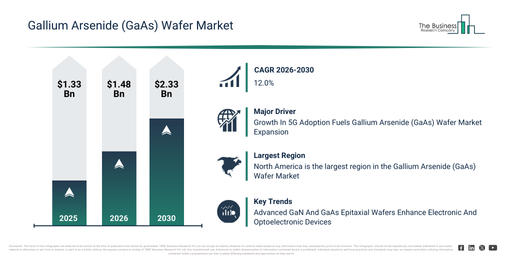
The gallium arsenide (gaas) wafer market has experienced rapid expansion in recent years. It is projected to climb from $1.33 billion in 2025 to $1.48 billion in 2026, indicating a compound annual growth rate (CAGR) of 11.8%. The increase observed in previous periods is largely attributable to the integration of gaas in microwave electronics, the proliferation of RF and wireless communication devices, advancements in LED and laser technologies, the need for high-speed semiconductor materials, and its utilization in defense electronics.
The gallium arsenide (gaas) wafer market size is anticipated to experience substantial growth over the next few years, with projections indicating it will reach $2.33 billion by 2030, achieving a compound annual growth rate (CAGR) of 12.0%. This expansion during the forecast period can be attributed to several factors, including the deployment of 5G and beyond networks, the rising adoption of VCSEL based sensing systems, the continued growth of electric and connected vehicles, the expansion of satellite communication systems, and an increasing demand for compound semiconductors. Prominent trends expected in this period encompass a growing demand for gaas wafers in high frequency RF applications, the rising adoption of gaas in optoelectronic and laser devices, an increasing use of gaas wafers in 5G and advanced communication systems, the expansion of gaas based devices in automotive electronics, and an intensified focus on high purity and low defect density gaas wafers.
Get A Free Sample Report With In-Depth Market Insights:
Gallium Arsenide (GaAs) Wafer Market Demand Drivers Opening New Revenue Streams
The increasing uptake of 5G infrastructure is anticipated to drive expansion within the gallium arsenide (GaAs) wafer market in the future. 5G infrastructure encompasses the necessary hardware and technological components for the fifth generation of mobile networks, providing enhanced data speeds, minimal latency, and simultaneous connectivity for many devices. This surge in 5G infrastructure adoption is fueled by the escalating demand for rapid internet, the widespread growth of connected devices, and the necessity for more dependable and efficient communication networks. GaAs wafers are instrumental in 5G infrastructure, facilitating the high-frequency signal processing vital for the quick data speeds and improved performance of 5G networks. For instance, in September 2023, according to 5G Americas, a US-based industry trade organization, North America’s 5G penetration rate reached an exceptional 40 percent, with a growth rate of 25.5% in the first half of 2023. Moreover, projections indicate North America’s 5G connections will reach a remarkable 669 million by 2028. Consequently, the expanding adoption of 5G infrastructure is propelling the growth of the gallium arsenide (GaAs) wafer market going forward.
Gallium Arsenide (GaAs) Wafer Market Segment Breakdown: Which Categories Lead On Revenue?
The gallium arsenide (gaas) wafer market covered in this report is segmented –
1) By Type: Vertical Gradient Freeze Gallium Arsenide (GaAs), Liquid-Encapsulated Czochralski Gallium Arsenide (GaAs), Other Types
2) By Application: Radio Frequency, Light Emitting Diode, Vertical-Cavity Surface-Emitting Laser (VCSEL), Photovoltaic
3) By End-Use: Telecommunication, Consumer Devices, Aerospace, Defense And Satcom, Automotive, Community Antenna Television (CATV) And Wired Broadband, Other End-Users
Subsegments:
1) By Vertical Gradient Freeze Gallium Arsenide (GaAs): High Purity Gaas Wafer, Low Defect Density Gaas Wafer, High-Performance Gaas For Optoelectronic Applications
2) By Liquid-Encapsulated Czochralsky Gallium Arsenide (GaAs): Czochralsky Gaas Wafers For Semiconductor Devices, Gaas For High-Speed Electronics, Gaas For Microwave And Rf Applications
3) By Other Types: Horizontal Gradient Freeze Gaas, Epitaxial Gaas Wafers, Gaas For Photovoltaic Applications, Gaas For Photonics And Laser Technology
Gallium Arsenide (GaAs) Wafer Market Trends Powering Strategic Industry Growth
Major companies operating within the gallium arsenide (GaAs) wafer market are prioritizing advanced technologies, including epitaxial gallium nitride (GaN) and gallium arsenide (GaAs) wafers, to improve the performance and efficiency of electronic and optoelectronic devices. Epitaxial GaN and GaAs wafers are slender semiconductor layers used in electronic and optical applications. As an illustration, in May 2023, IQE, a UK-based epiwafer foundry company, introduced a 200mm RGB epi for micro-LED display qualification. These wafers incorporate gallium nitride (GaN) and gallium arsenide (GaAs) and are specifically engineered for micro-LED displays. This innovation is crucial for new display technologies in wearables, augmented reality (AR) or virtual reality (VR) headsets, and large screens.
Gallium Arsenide (GaAs) Wafer Market Leading Players And Competitive Positioning
Major companies operating in the gallium arsenide (gaas) wafer market are AXT Inc., IQE PLC, WIN Semiconductors Corp., IntelliEPI Inc., Wafer Technology Ltd., Freiberger Compound Materials GmbH, Vital Materials Co. Ltd., Xiamen Powerway Advanced Material Co., Ltd., Xinxiang Shenzhou Crystal Technology Co., Ltd., Sumitomo Electric Device Innovations Inc., Compound Semiconductor Technologies Global Ltd., LandMark Optoelectronics Corporation, San’an Optoelectronics Co., Ltd., Qingdao Jiaying Semiconductor Co., Ltd., Mitsubishi Chemical Group, Hitachi Cable Fine Tech Ltd., Sumitomo Chemical Co., Ltd., Wafer Works Corporation, EpiWorks Inc., Ommic SAS.
View The Full Gallium Arsenide (GaAs) Wafer Market Report:
Gallium Arsenide (GaAs) Wafer Market Regional Analysis: Which Geography Leads On Revenue?
North America was the largest region in the gallium arsenide (GaAs) wafer market in 2025. Asia-Pacific is expected to be the fastest-growing region in the forecast period. The regions covered in the gallium arsenide (gaas) wafer market report are Asia-Pacific, South East Asia, Western Europe, Eastern Europe, North America, South America, Middle East, Africa.
Reach Out To Our Team:
The Business Research Company: https://www.thebusinessresearchcompany.com/
Americas: +1 310-496-7795
Asia: +44 7882 955267 & +91 8897263534
Europe: +44 7882 955267
Email us at: marketing@tbrc.info
Follow us on:
LinkedIn: https://in.linkedin.com/company/the-business-research-company
YouTube: https://www.youtube.com/channel/UC24_fI0rV8cR5DxlCpgmyFQ
Global Market Model: https://www.thebusinessresearchcompany.com/global-market-model

Wasay has over a decade of experience in market research, data modelling, and analytics, with prior experience at GlobalData and Decision Tree Consulting Services. At The Business Research Company , he leads research operations across syndicated studies, customized consulting engagements, and the Global Market Model platform. His professional experience includes supporting organizations such as Boston Consulting Group, KPMG, and Ernst & Young. Wasay holds a degree in Electronics and Communications Engineering, postgraduate management qualifications from International Management Institute Belgium and Indian School of Business and Entrepreneurship, and completed the Integrated Program in Business Analytics from Indian Institute of Management Indore.