
Built to provide research that’s more actionable and strategically valuable, The Business Research Company’s 2026 market reports include market attractiveness analysis, total addressable market sizing, company benchmarking matrices, interactive Excel dashboards, broader supply chain intelligence, emerging startup tracking, and in-depth product insights.
Semiconductor Deposition Material Market Value Growth And Long-Term Outlook
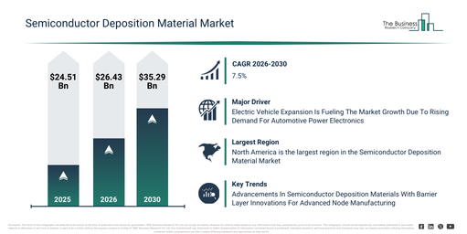
The semiconductor deposition material market size has experienced significant expansion over recent years. Its projected growth will see it rise from $24.51 billion in 2025 to $26.43 billion in 2026, advancing at a compound annual growth rate (CAGR) of 7.8%. In the past, this market’s growth was primarily due to the increase in semiconductor manufacturing, the rising adoption of ICs and memory devices, the initial implementation of PVD and CVD techniques, heightened demand for consumer electronics, and the expansion within automotive electronics.
The semiconductor deposition material market size is anticipated to experience substantial expansion over the upcoming years. By 2030, this market is projected to reach $35.29 billion, demonstrating a compound annual growth rate (CAGR) of 7.5%. Factors driving this expansion during the forecast period include the rise of sophisticated IC fabrication methods, the increasing use of ALD in developing high-performance devices, the growth within power electronics and optoelectronics, significant demand from the automotive and aerospace industries, and breakthroughs in compound semiconductor materials. Key trends anticipated during this period encompass the increasing integration of atomic layer deposition for producing accurate thin films, a heightened need for highly pure semiconductor deposition materials, the expanding application of metals, oxides, and nitrides in device manufacturing, a greater incorporation of deposition materials in memory and power applications, and a stronger inclination towards sophisticated deposition methods such as plasma-enhanced and spatial ALD.
Get A Free Sample Report With In-Depth Market Insights:
Semiconductor Deposition Material Market Demand Drivers: What’s Powering Industry Growth?
The growth in electric vehicles is anticipated to drive the semiconductor deposition material market throughout the projection period. Electric vehicles are automobiles powered by electric motors and battery systems, which require power management integrated circuits, battery management systems, and motor control semiconductors for efficient operation. The increasing adoption of electric vehicles has been propelled by rapidly declining battery costs, making EVs more accessible and encouraging consumers to transition from conventional fuel-powered vehicles. Semiconductor deposition materials are crucial for electric vehicles, facilitating the creation of high-performance power electronics and control chips that enhance battery management, charging efficiency, and overall vehicle performance. For instance, in May 2025, according to the International Energy Agency, a France-based intergovernmental organization, over 4 million EVs were sold worldwide, representing a 35% increase compared to the same period in 2024. Projections further indicate that over 20 million new electric cars will be sold by the end of 2025, a 25% year-on-year increase from 17 million EVs sold in 2024. Consequently, the expansion of electric vehicles is significantly fueling the semiconductor deposition material market.
Semiconductor Deposition Material Market Segment Outlook: Which Categories Are Growing Fastest?
The semiconductor deposition material market covered in this report is segmented –
1) By Type: Physical Vapor Deposition (PVD), Chemical Vapor Deposition (CVD), Atomic Layer Deposition (ALD), Electrochemical Deposition
2) By Material Composition: Metals, Oxides, Nitrides, Polymer-Based Materials, Silicon-Based Materials, Compound Semiconductors
3) By Deposition Technique: Chemical Vapor Deposition, Physical Vapor Deposition, Atomic Layer Deposition, Other Deposition Techniques
4) By Application: Integrated Circuits (ICs), Memory Devices, Power Devices, Optoelectronic Devices, Light Emitting Diodes And Laser Diodes, Semiconductor Packaging
5) By End-Use Industry: Consumer Electronics, Telecommunications, Aerospace And Defense, Automotive, Healthcare, Industrial Automation
Subsegments:
1) By Physical Vapor Deposition (PVD): Sputtering, Evaporation, Cathodic Arc Deposition, Pulsed Laser Deposition, Molecular Beam Epitaxy
2) By Chemical Vapor Deposition (CVD): Plasma Enhanced Chemical Vapor Deposition, Low Pressure Chemical Vapor Deposition, Atmospheric Pressure Chemical Vapor Deposition, Metal Organic Chemical Vapor Deposition, Atomic Layer Deposition
3) By Atomic Layer Deposition (ALD): Thermal Atomic Layer Deposition, Plasma-Enhanced Atomic Layer Deposition, Spatial Atomic Layer Deposition, Thermal Spatial Atomic Layer Deposition, Radical-Enhanced Atomic Layer Deposition
4) By Electrochemical Deposition: Copper, Nickel, Gold, Silver, Cobalt, Platinum, Palladium, Ruthenium, Rhodium, Alloy
Semiconductor Deposition Material Market Innovation Trends: What Developments Are Reshaping The Industry?
Leading companies engaged in the semiconductor deposition material market are concentrating on advancements in barrier materials, which includes developing sophisticated barrier layers with significantly improved characteristics for extreme ultraviolet (EUV) lithography and upcoming chip architectures. These cutting-edge materials are designed to offer superior protection against moisture, oxygen, and chemical contamination, thereby safeguarding the structural integrity and performance of ultra-thin device layers at nanoscale. For instance, in May 2023, Merck KGaA, a Germany-based prominent science and technology company, unveiled a new line of advanced barrier materials specifically for semiconductor applications. These materials are engineered to provide exceptional impermeability, enabling the creation of thinner film stacks without compromising reliability, thus supporting the transition to sub-3 nm nodes and advanced 3D device structures. This innovation enhances process uniformity, film adhesion, and long-term device stability, leading to a substantial improvement in yield rates for logic and memory manufacturers. Furthermore, these barrier materials are fully compatible with existing chemical vapor deposition (CVD) and atomic layer deposition (ALD) tools, facilitating seamless integration into current semiconductor fabrication workflows.
Semiconductor Deposition Material Market Leading Companies And Competitive Benchmarking
Major companies operating in the semiconductor deposition material market are Shin-Etsu Chemical Co. Ltd., Merck KGaA, JSR Corporation, Fujifilm Electronic Materials Co. Ltd., Dow Inc., Entegris Inc., Air Products and Chemicals Inc., Air Liquide S.A., Linde plc, SK Materials Co. Ltd., Evonik Industries AG, Wacker Chemie AG, Mitsubishi Chemical Corporation, ADEKA Corporation, Tanaka Kikinzoku Group, Materion Corporation, Soulbrain Co. Ltd., Kanto Chemical Co. Inc., Honeywell International Inc., Plansee Group, Cabot Microelectronics Corporation, and Sumitomo Chemical Co. Ltd.
View The Full Semiconductor Deposition Material Market Report:
Semiconductor Deposition Material Market Geographic Landscape: Which Region Leads Industry Growth?
North America was the largest region in the semiconductor deposition material market in 2025. Asia-Pacific is expected to be the fastest-growing region in the forecast period. The regions covered in the semiconductor deposition material market report are Asia-Pacific, South East Asia, Western Europe, Eastern Europe, North America, South America, Middle East, Africa.
Reach Out To Our Team:
The Business Research Company: https://www.thebusinessresearchcompany.com/
Americas: +1 310-496-7795
Asia: +44 7882 955267 & +91 8897263534
Europe: +44 7882 955267
Email us at: marketing@tbrc.info
Follow us on:
LinkedIn: https://in.linkedin.com/company/the-business-research-company
YouTube: https://www.youtube.com/channel/UC24_fI0rV8cR5DxlCpgmyFQ
Global Market Model: https://www.thebusinessresearchcompany.com/global-market-model

Wasay has over a decade of experience in market research, data modelling, and analytics, with prior experience at GlobalData and Decision Tree Consulting Services. At The Business Research Company , he leads research operations across syndicated studies, customized consulting engagements, and the Global Market Model platform. His professional experience includes supporting organizations such as Boston Consulting Group, KPMG, and Ernst & Young. Wasay holds a degree in Electronics and Communications Engineering, postgraduate management qualifications from International Management Institute Belgium and Indian School of Business and Entrepreneurship, and completed the Integrated Program in Business Analytics from Indian Institute of Management Indore.