Built to provide research that’s more actionable and strategically valuable, The Business Research Company’s 2026 market reports include market attractiveness analysis, total addressable market sizing, company benchmarking matrices, interactive Excel dashboards, broader supply chain intelligence, emerging startup tracking, and in-depth product insights.
Semiconductor Metrology And Inspection Market Revenue Outlook: What CAGR Lies Ahead Through 2030?
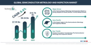
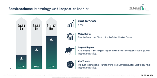
The semiconductor metrology and inspection market has seen substantial growth in its size over recent years. Its value is expected to rise from $8.34 billion in 2025 to $8.88 billion in 2026, achieving a compound annual growth rate (CAGR) of 6.5%. This market’s expansion during the past period can be linked to the rising demand for precise inspection processes in lithography, the increasing complexity of semiconductor device geometries, a greater need for wafer defect detection, the wider application of thin-film metrology, and developments in e-beam inspection platforms.
The semiconductor metrology and inspection market is projected to experience substantial expansion in the coming years, with its size anticipated to reach $11.47 billion by 2030, exhibiting a compound annual growth rate (CAGR) of 6.6%. This growth during the forecast period is primarily fueled by factors such as the increasing manufacture of advanced nodes smaller than 5nm, a heightened demand for automated high-throughput metrology, the broadening scope of 3D packaging inspection requirements, greater reliance on AI-powered inspection analytics, and a surge in global investment for semiconductor fabrication plants. Furthermore, significant trends expected over this period include advancements in AI-driven defect detection, the integration of intelligent semiconductor manufacturing, the proliferation of cloud-enabled inspection systems, the broadening of connected metrology platforms, and the development of autonomous wafer inspection solutions.
Get A Free Sample Report With In-Depth Market Insights:
Semiconductor Metrology And Inspection Market Demand Drivers Opening New Revenue Streams
The increasing prevalence of consumer electronics is projected to boost the semiconductor metrology and inspection market moving forward. The heightened demand for semiconductors in devices like smartphones and IoT gadgets necessitates highly precise manufacturing processes. Rigorous quality standards for consumer electronics compel the adoption of advanced metrology tools for defect detection. Miniaturization trends in electronics call for accurate measurement procedures, and innovations in consumer electronics technology rely on continuous improvements in semiconductor manufacturing capabilities. For example, in May 2023, the Japan Electronics and Information Technology Industries Association, a Japan-based trade association, reported that the total electronic equipment production in Japan reached 771,457 units. Additionally, consumer electronics production hit 32,099 units in May 2023, an increase from 25,268 units in May 2022. This demonstrates how the growth in consumer electronics is propelling the semiconductor metrology and inspection market.
Semiconductor Metrology And Inspection Market Segment Breakdown: Which Categories Lead On Revenue?
The semiconductor metrology and inspection market covered in this report is segmented –
1) By Type: Optical, E-Beam
2) By Lithography Metrology: Overlay, Dimension Equipment, Mask Inspection And Metrology
3) By Application: Lithography Metrology, Wafer Inspection, Thin Film Metrology
Subsegments:
1) By Optical: Optical Inspection Systems, Scatterometry, Interferometry, Reflective Measurement Systems
2) By E-Beam: E-Beam Inspection Systems, E-Beam Metrology Systems, E-Beam Lithography Tools
Semiconductor Metrology And Inspection Market Trends Powering Strategic Industry Growth
Leading companies in the semiconductor metrology and inspection market are concentrating on developing innovative technologies to refine the inspection process and uphold the quality of semiconductor devices. As an example, in March 2024, Hitachi High-Tech Corporation, a Japan-based manufacturer of advanced technology equipment, launched the LS9300AD wafer inspection system. This system is distinguished by a built-in Differential Interference Contrast (DIC) optical system for highly sensitive detection of minuscule defects, a DIC-compatible data processing system that allows for concurrent dark-field laser scattering and DIC inspection mapping, and a true wafer-edge-grip method facilitating both front and back surface inspection of non-patterned wafers. This particular innovation boosts Hitachi High-Tech’s position and offerings in the semiconductor metrology and inspection market.
Semiconductor Metrology And Inspection Market Leading Players And Competitive Positioning
Major companies operating in the semiconductor metrology and inspection market are KLA Corporation, Applied Materials Inc., Onto Innovation Inc. (Rudolph Technologies Corporation), Thermo Fisher Scientific Inc., Hitachi High-Tech Corporation, Nova Measuring Instruments Ltd., ASML Holding NV, Lasertec Corporation, JEOL Ltd., Nikon Metrology NV, Camtek Limited, Bruker Corporation, Nanometrics Incorporated, Horiba Ltd., Carl Zeiss AG, SENTECH Instruments GmbH, Keyence Corporation, Accurion GmbH, Alicona Imaging GmbH, Veeco Instruments Inc., FormFactor Inc.
View The Full Semiconductor Metrology And Inspection Market Report:
Semiconductor Metrology And Inspection Market Regional Analysis: Which Geography Leads On Revenue?
Asia-Pacific was the largest region in the semiconductor metrology and inspection market in 2025. Asia-Pacific is expected to be the fastest-growing region in the forecast period. The regions covered in the semiconductor metrology and inspection market report are Asia-Pacific, South East Asia, Western Europe, Eastern Europe, North America, South America, Middle East, Africa.
Reach Out To Our Team:
The Business Research Company: https://www.thebusinessresearchcompany.com/
Americas: +1 310-496-7795
Asia: +44 7882 955267 & +91 8897263534
Europe: +44 7882 955267
Email us at: marketing@tbrc.info
Follow us on:
LinkedIn: https://in.linkedin.com/company/the-business-research-company
YouTube: https://www.youtube.com/channel/UC24_fI0rV8cR5DxlCpgmyFQ
Global Market Model: https://www.thebusinessresearchcompany.com/global-market-model

Wasay has over a decade of experience in market research, data modelling, and analytics, with prior experience at GlobalData and Decision Tree Consulting Services. At The Business Research Company , he leads research operations across syndicated studies, customized consulting engagements, and the Global Market Model platform. His professional experience includes supporting organizations such as Boston Consulting Group, KPMG, and Ernst & Young. Wasay holds a degree in Electronics and Communications Engineering, postgraduate management qualifications from International Management Institute Belgium and Indian School of Business and Entrepreneurship, and completed the Integrated Program in Business Analytics from Indian Institute of Management Indore.