
Built to provide research that’s more actionable and strategically valuable, The Business Research Company’s 2026 market reports include market attractiveness analysis, total addressable market sizing, company benchmarking matrices, interactive Excel dashboards, broader supply chain intelligence, emerging startup tracking, and in-depth product insights.
Wafer Bonder And Debonder Market CAGR Outlook And Future Development
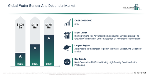
The wafer bonder and debonder market size has demonstrated significant growth over recent years. This market is anticipated to expand from $1.06 billion in 2025 to $1.16 billion in 2026, achieving a compound annual growth rate (CAGR) of 9.4%. The historical expansion can be attributed to several factors including the rise of semiconductor fabrication, the increased adoption of MEMS devices, the necessity for wafer thinning processes, ongoing advancements in bonding technologies, and a surge in the production of electronic devices.
The wafer bonder and debonder market size is anticipated to experience robust expansion over the coming years. This market is projected to reach $1.61 billion by 2030, demonstrating a compound annual growth rate (CAGR) of 8.5%. Key factors driving this growth during the forecast period include the proliferation of advanced packaging technologies, an escalating demand for power semiconductors, the expansion of electronics within electric vehicles, the ongoing trend of semiconductor miniaturization, and significant investments in high-volume wafer manufacturing. Significant trends observed for this period encompass the wider embrace of advanced wafer bonding processes, an increasing need for precision alignment and debonding without damage, greater application in sophisticated semiconductor packaging, the broadening scope of MEMS and sensor manufacturing, and an enhanced emphasis on automated high-volume wafer bonding.
Get A Free Sample Report With In-Depth Market Insights:
Wafer Bonder And Debonder Market Development Factors: What’s Supporting Demand?
The future expansion of the wafer bonder and debonder market is anticipated to be driven by the rising need for sophisticated semiconductor devices. These devices are defined as electronic parts that harness the electrical characteristics of semiconductor substances to manage electric current movement. This heightened demand for advanced semiconductors primarily stems from the quick integration of new technologies, including artificial intelligence (AI), the internet of things (IOT), and fifth-generation (5G) wireless technology, all of which necessitate enhanced processing speeds and greater energy effectiveness. In the manufacturing of semiconductor devices, wafer bonders and debonders play a crucial role by facilitating the accurate joining and detachment of wafers during intricate packaging and production stages. A relevant example is that, in July 2024, data from the Semiconductor Industry Association, a US trade body, indicated that worldwide semiconductor sales hit $49.1 billion in May 2024. This figure marked a 19.3% year-on-year rise from $41.2 billion in May 2023 and showed a 4.1% month-on-month increase over $47.2 billion in April 2024. Consequently, the expanding need for advanced semiconductor devices is fueling the expansion of the wafer bonder and debonder market.
Wafer Bonder And Debonder Market Segment Analysis: What Are The Core Market Categories?
The wafer bonder and debonder market covered in this report is segmented –
1) By Type: Manual Wafer Bonders, Semi-Automatic Wafer Bonders, Fully Automatic Wafer Bonders
2) By Technology: Eutectic Bonding, Anodic Bonding, Fusion Bonding, Adhesive Bonding, Other Technologies
3) By Application: Micro-Electro-Mechanical Systems (MEMS) Devices, Power Devices, Optoelectronic Devices, Radio Frequency (RF) Devices, Interposers, Other Applications
4) By End-Use: Semiconductor, Electronics Automotive: Healthcare, Telecommunications, Other End Uses
Subsegments:
1) By Manual Wafer Bonders: Research And Development Bonding, Low-Volume Production Bonding, Prototype Device Bonding
2) By Semi-Automatic Wafer Bonders: Small-Scale Production Bonding, Pilot Line Applications, Academic And Laboratory Bonding
3) By Fully Automatic Wafer Bonders: High-Volume Manufacturing Bonding, Advanced Packaging Bonding, Micro-Electro-Mechanical Systems (MEMS) And Sensor Mass Production
Wafer Bonder And Debonder Market Trends Powering Strategic Industry Growth
Major companies operating in the wafer bonder and debonder market are concentrating on creating innovative solutions, including automated die-to-wafer (D2W) hybrid bonding systems, to improve precision, scalability, and throughput in advanced semiconductor packaging and 3D integration applications. An automated die-to-wafer (D2W) hybrid bonding system refers to sophisticated semiconductor equipment that enables the exact alignment and bonding of individual dies onto a wafer, employing both mechanical and electrical chemical interconnections for high-density 3D integration. For instance, in May 2025, SUSS MicroTec SE, a Germany-based manufacturer of equipment and process solutions for microstructuring, introduced the XBC300 Gen2 D2W platform, a custom bonding solution that enhances the company’s hybrid bonding portfolio. This new platform solidifies SUSS’s position as a market leader in providing a fully integrated D2W hybrid bonding solution for stringent manufacturing requirements. The updated SUSS process solution facilitates die-to-wafer (D2W) bonding on 200 mm and 300 mm substrates and fulfills the most demanding inter-die spacing specifications. It stands as an ideal platform for producing high-precision chips, thanks to industry-leading footprint savings of up to 40% and a post-bond accuracy of < ±200 nm.
Wafer Bonder And Debonder Market Top Companies Driving Competitive Growth
Major companies operating in the wafer bonder and debonder market are Canon Inc., Applied Materials Inc., Tokyo Electron Limited, Nitto Denko Corporation, ASM Pacific Technology Ltd., Shibaura Mechatronics Corporation, SÜSS MicroTec SE, EV Group, Palomar Technologies Inc., Toray Engineering Co. Ltd., Bondtech Co. Ltd., Applied Microengineering Ltd., Shanghai Micro Electronics Equipment Co. Ltd., Hybond Inc., SiSTEM Technology Ltd., Ayumi Industry Co. Ltd., Disco Corporation, Tokyo Seimitsu Co. Ltd., FINEPLACER, Test Research Inc., EVG Group, DNP
View The Full Wafer Bonder And Debonder Market Report:
Wafer Bonder And Debonder Market Top Region By Revenue And Market Share
Asia-Pacific was the largest region in the wafer bonder and debonder market in 2025, and it is expected to be the fastest-growing region in the forecast period. The regions covered in the wafer bonder and debonder market report are Asia-Pacific, South East Asia, Western Europe, Eastern Europe, North America, South America, Middle East, Africa
Reach Out To Our Team:
The Business Research Company: https://www.thebusinessresearchcompany.com/
Americas: +1 310-496-7795
Asia: +44 7882 955267 & +91 8897263534
Europe: +44 7882 955267
Email us at: marketing@tbrc.info
Follow us on:
LinkedIn: https://in.linkedin.com/company/the-business-research-company
YouTube: https://www.youtube.com/channel/UC24_fI0rV8cR5DxlCpgmyFQ
Global Market Model: https://www.thebusinessresearchcompany.com/global-market-model

Wasay has over a decade of experience in market research, data modelling, and analytics, with prior experience at GlobalData and Decision Tree Consulting Services. At The Business Research Company , he leads research operations across syndicated studies, customized consulting engagements, and the Global Market Model platform. His professional experience includes supporting organizations such as Boston Consulting Group, KPMG, and Ernst & Young. Wasay holds a degree in Electronics and Communications Engineering, postgraduate management qualifications from International Management Institute Belgium and Indian School of Business and Entrepreneurship, and completed the Integrated Program in Business Analytics from Indian Institute of Management Indore.