
Featuring market attractiveness scoring, total addressable market sizing, company benchmarking matrices, interactive Excel dashboards, deeper supply chain intelligence, emerging startup tracking, and granular product-level insights, The Business Research Company’s 2026 market reports are built to deliver research that is both more actionable and more strategically valuable.
Semiconductor Dielectric Etching Equipment Market Forecast: Value Set To Climb From $4.86 Billion To $6.82 Billion
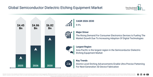
The market size for semiconductor dielectric etching equipment has demonstrated robust expansion recently. This market is projected to expand from $4.45 billion in 2025 to $4.86 billion in 2026, exhibiting a compound annual growth rate (CAGR) of 9.3%. Historically, this expansion has been driven by factors such as an escalating demand for semiconductors originating from consumer electronics, the enlargement of integrated circuit manufacturing capabilities, the increasing embrace of advanced semiconductor nodes, rising capital expenditures in semiconductor fabrication plants, and a heightened need for smaller electronic components.
The semiconductor dielectric etching equipment market size is projected to experience robust expansion over the coming years. It is expected to grow to $6.82 billion in 2030, exhibiting a compound annual growth rate (CAGR) of 8.9%. This anticipated growth during the forecast period is attributable to the increasing demand for high performance computing chips, rising production of advanced memory and logic devices, a growing adoption of 3D semiconductor architectures, expanding investments in semiconductor manufacturing across various regions, and the increasing need for precise dielectric layer patterning technologies. Significant trends within this forecast period include the increasing adoption of advanced plasma etching technologies for semiconductor fabrication, a growing demand for atomic layer etching equipment in advanced node manufacturing, the rising integration of high precision dielectric etching processes for miniaturized IC designs, an increasing development of high throughput etching equipment for large scale wafer production, and a growing focus on enhanced process control and uniformity in semiconductor etching operations.
Get A Free Sample Report With In-Depth Market Insights:
Semiconductor Dielectric Etching Equipment Market Growth Catalysts And Demand Drivers
The semiconductor dielectric etching equipment market is projected to grow due to the increasing demand for consumer electronics devices. These devices refer to electronic products designed for everyday personal or household use, encompassing items such as smartphones, laptops, tablets, wearables, and smart home systems. The heightened demand for consumer electronics devices is fueled by advancements in digital connectivity, as a growing number of individuals and businesses rely on internet-enabled technology for communication, work, entertainment, and various smart applications. Semiconductor dielectric etching equipment enables the precise removal of dielectric materials at a nanoscale, facilitating the creation of highly miniaturized, high-performance chips that power consumer electronics devices like smartphones, laptops, wearables, and smart home systems. For example, in May 2023, the Japan Electronics and Information Technology Industries Association, a Japan-based trade association, reported that Japan’s consumer electronic equipment production reached 32,099 million yen (approximately USD 198.92 million), an increase from 24,960 million yen (about USD 154.68 million) recorded in May 2022. Therefore, the escalating demand for consumer electronics devices is a key driver for the expansion of the semiconductor dielectric etching equipment market.
Semiconductor Dielectric Etching Equipment Market Segment Analysis: What Are The Core Market Categories?
The semiconductor dielectric etching equipment market covered in this report is segmented –
1) By Type: Wet Etching Equipment, Dry Etching Equipment
2) By Installation: Clean Room, Laboratory, Production Floor, Pilot Plant
3) By Wafer Size: Less Than 200 Millimeters, 200 Millimeters To 300 Millimeters, Above 300 Millimeters
4) By Application: Logic Devices, Memory Devices, Power Devices, Analog And Radio Frequency Devices, Microelectromechanical Systems, Sensors
5) By End User: Foundries, Integrated Device Manufacturers, Research Institutions, Original Equipment Manufacturers
Subsegments:
1) By Wet Etching Equipment: Chemical Wet Etching Equipment, Spray Wet Etching Equipment, Immersion Wet Etching Equipment, Single Wafer Wet Etching Equipment, Batch Wet Etching Equipment
2) By Dry Etching Equipment: Reactive Ion Etching Equipment, Inductively Coupled Plasma Etching Equipment, Capacitively Coupled Plasma Etching Equipment, Deep Reactive Ion Etching Equipment, Atomic Layer Etching Equipment, Plasma Etching Equipment, Cryogenic Etching Equipment
Semiconductor Dielectric Etching Equipment Market Trends Shaping Long-Term Demand
Leading companies in the **semiconductor dielectric etching equipment market** are prioritizing technological advancements, such as **atomic-level dielectric etching systems**, to achieve ultra-precise patterning, enhance process control in advanced 3D device manufacturing, and support continuous device scaling at nanometer and sub-nanometer nodes. These **atomic-level dielectric etching systems** represent sophisticated semiconductor manufacturing tools that meticulously remove dielectric materials with extreme precision at the atomic scale, offering superior process control, reduced material damage, and improved pattern fidelity when compared to conventional plasma etching technologies. For instance, in **November 2024**, **Hitachi High-Tech Corporation**, a **Japan**-based semiconductor equipment manufacturer, unveiled the **DCR Etch System 9060 Series**, an innovative dry chemical removal etching system tailored for advanced three-dimensional semiconductor device manufacturing. This system allows for atomic-level isotropic etching and precise material removal, catering to complex device structures, including **3D NAND** and **advanced memory applications**. It incorporates proprietary plasma processing technology, which helps to improve etch uniformity, process stability, and manufacturing efficiency while concurrently minimizing damage to surrounding materials. This solution is crucial for supporting increasingly intricate semiconductor architectures that demand precise dielectric layer processing and enhanced device performance.
Semiconductor Dielectric Etching Equipment Market Top Companies Driving Competitive Growth
Major companies operating in the semiconductor dielectric etching equipment market are Applied Materials Inc., Tokyo Electron Limited, Lam Research Corporation, Hitachi High-Tech Corporation, NAURA Technology Group Co. Ltd., SCREEN Semiconductor Solutions Co. Ltd., Advanced Micro-Fabrication Equipment Inc. China, SEMES Co. Ltd., ULVAC Inc., Mattson Technology Inc., Oxford Instruments plc, Shibaura Mechatronics Corporation, Canon Anelva Corporation, Plasma-Therm LLC, GigaLane Co. Ltd., Samco Inc., Sentech Instruments GmbH, Plasma Etch Inc.
View The Full Semiconductor Dielectric Etching Equipment Market Report:
Semiconductor Dielectric Etching Equipment Market Top Region: Where Does Most Revenue Come From?
Asia-Pacific was the largest region in the semiconductor dielectric etching equipment market in 2025. North America is expected to be the fastest-growing region in the forecast period. The regions covered in the semiconductor dielectric etching equipment market report are Asia-Pacific, South East Asia, Western Europe, Eastern Europe, North America, South America, Middle East, Africa.
Reach Out To Our Team:
The Business Research Company: https://www.thebusinessresearchcompany.com/
Americas: +1 310-496-7795
Asia: +44 7882 955267 & +91 8897263534
Europe: +44 7882 955267
Email us at: marketing@tbrc.info
Follow us on:
LinkedIn: https://in.linkedin.com/company/the-business-research-company
YouTube: https://www.youtube.com/channel/UC24_fI0rV8cR5DxlCpgmyFQ
Global Market Model: https://www.thebusinessresearchcompany.com/global-market-model

Wasay has over a decade of experience in market research, data modelling, and analytics, with prior experience at GlobalData and Decision Tree Consulting Services. At The Business Research Company , he leads research operations across syndicated studies, customized consulting engagements, and the Global Market Model platform. His professional experience includes supporting organizations such as Boston Consulting Group, KPMG, and Ernst & Young. Wasay holds a degree in Electronics and Communications Engineering, postgraduate management qualifications from International Management Institute Belgium and Indian School of Business and Entrepreneurship, and completed the Integrated Program in Business Analytics from Indian Institute of Management Indore.