
Built to provide research that’s more actionable and strategically valuable, The Business Research Company’s 2026 market reports include market attractiveness analysis, total addressable market sizing, company benchmarking matrices, interactive Excel dashboards, broader supply chain intelligence, emerging startup tracking, and in-depth product insights.
Fin Field Effect Transistor (FinFET) Wafer Foundry Market Revenue Growth On Track For A 8.2% CAGR Through 2030
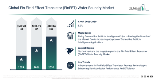
The fin field effect transistor (finfet) wafer foundry market size has seen significant expansion over recent years. It is anticipated to increase from $53.93 billion in 2025 to $58.59 billion in 2026, exhibiting a compound annual growth rate (CAGR) of 8.6%. This historical growth can be attributed to factors such as increased semiconductor demand, the growing adoption of smartphones and mobile processors, the expansion of data center infrastructure, a rising need for advanced processors, and the growth within automotive electronics.
The fin field effect transistor (finfet) wafer foundry market size is projected to experience robust expansion over the coming years. This market is set to reach $80.34 billion by 2030, exhibiting a compound annual growth rate (CAGR) of 8.2%. The anticipated growth during this period stems from factors such as increasing demand for AI accelerators, rising needs for high-performance computing, the expansion of advanced-node semiconductor manufacturing, growing demand for automotive SoCs, and an increase in semiconductor content within connected devices. Key developments expected during the forecast span involve the increasing adoption of advanced FinFET process nodes, a growing need for high-performance semiconductor manufacturing, rising investment in advanced foundry capacity, an increasing requirement for customized semiconductor fabrication, and the growing integration of 3D transistor architectures.
Get A Free Sample Report With In-Depth Market Insights:
Fin Field Effect Transistor (FinFET) Wafer Foundry Market Development Factors: What’s Supporting Demand?
The increasing need for artificial intelligence chips is projected to stimulate expansion in the fin field effect transistor (FinFET) wafer foundry market. Artificial intelligence chips are specialized semiconductor devices engineered to accelerate AI tasks like machine learning, deep learning, and neural network processing with high computational efficiency. The escalating adoption of generative artificial intelligence applications is driving the surge in demand for these chips. This heightened demand for artificial intelligence chips, in turn, boosts the requirement for FinFET wafer foundry services, as AI processors depend on advanced FinFET transistor architectures for superior computing performance, enhanced power efficiency, and greater transistor density essential for complex AI workloads. For instance, in June 2026, according to the Semiconductor Industry Association (SIA), semiconductors accounted for over 95% of the content value in a leading artificial intelligence (AI) data server rack, with each AI server rack containing more than 4,500 packaged chips. Consequently, the rising demand for artificial intelligence chips is a key driver for the growth of the fin field effect transistor (FinFET) wafer foundry market.
Fin Field Effect Transistor (FinFET) Wafer Foundry Market Segmentation And Category Overview
The fin field effect transistor (finfet) wafer foundry market covered in this report is segmented –
1) By Product Type: Central Processing Unit, Field Programmable Gate Array, Graphics Processing Unit, System On Chip, Microcontroller Unit, Network Processors, Other Types
2) By Fin Field Effect Transistor Process Node: 14 Nanometer Fin Field Effect Transistor Technology, 7 Nanometer Fin Field Effect Transistor Technology, 5 Nanometer Fin Field Effect Transistor Technology, 3 Nanometer Fin Field Effect Transistor Technology
3) By Technology Type: Bulk Fin Field Effect Transistor, Silicon On Insulator Fin Field Effect Transistor, Fully Depleted Silicon On Insulator Fin Field Effect Transistor
4) By End User Industry: Telecommunications, Automotive, Consumer Electronics, Industrial Electronics, Healthcare Devices
Subsegments:
1) By Central Processing Unit: Desktop Processor, Mobile Processor, Server Processor, Embedded Processor
2) By Field Programmable Gate Array: Low Density Field Programmable Gate Array, Mid Density Field Programmable Gate Array, High Density Field Programmable Gate Array, System On Module Field Programmable Gate Array
3) By Graphics Processing Unit: Integrated Graphics Processing Unit, Discrete Graphics Processing Unit, Data Center Graphics Processing Unit, Embedded Graphics Processing Unit
4) By System On Chip: Mobile System On Chip, Automotive System On Chip, Industrial System On Chip, Internet Of Things System On Chip
5) By Microcontroller Unit: Eight Bit Microcontroller Unit, Sixteen Bit Microcontroller Unit, Thirty Two Bit Microcontroller Unit, Automotive Microcontroller Unit
6) By Network Processors: Multi Core Network Processor, Packet Processing Network Processor, Communication Network Processor, Security Network Processor
7) By Other Types: Artificial Intelligence Accelerators, Digital Signal Processors, Application Specific Integrated Circuits, Security Processors
Fin Field Effect Transistor (FinFET) Wafer Foundry Market Transformation Trends: What Innovations Are Driving Change?
Leading companies within the fin field effect transistor (FinFET) wafer foundry market are concentrating on developing innovative solutions, such as fin field effect transistor process technologies, to boost transistor performance, decrease power consumption, increase chip density, and meet the growing demand for advanced semiconductor manufacturing across artificial intelligence, high-performance computing, automotive electronics, and mobile applications. FinFET process technologies are sophisticated semiconductor fabrication methods that utilize three-dimensional fin-shaped transistor structures, offering superior control over current flow compared to conventional planar transistors, which allows for higher performance and energy efficiency at smaller process nodes. For example, in May 2026, United Microelectronics Corporation (UMC), a Taiwan-based semiconductor foundry company, unveiled its 14nm embedded high-voltage (eHV) FinFET technology platform, an advanced wafer fabrication solution specifically designed for next-generation display driver integrated circuits (ICs). This platform is founded on Fin Field-Effect Transistor (FinFET) process technology, which incorporates three-dimensional transistor structures to enhance power efficiency, performance, and transistor density when compared with traditional planar transistor technologies. Validated at UMC’s Fab 12A, this technology empowers semiconductor manufacturers to create smaller, more power-efficient, and higher-performance display driver ICs for advanced display applications. The platform delivers improved electrical performance and reduced chip size, simultaneously supporting the increasing need for high-resolution smartphone displays and next-generation display technologies. By providing a validated FinFET-based manufacturing process complete with an available process design kit (PDK), UMC enables its customers to accelerate the development and production of advanced semiconductor devices.
Fin Field Effect Transistor (FinFET) Wafer Foundry Market Company Landscape And Competitive Strategy
Major companies operating in the fin field effect transistor (finfet) wafer foundry market are Taiwan Semiconductor Manufacturing Company Limited, Samsung Electronics Co. Ltd., Intel Corporation, United Microelectronics Corporation, GlobalFoundries Inc., Semiconductor Manufacturing International Corporation, Shanghai Huali Microelectronics Corporation, Sony Semiconductor Solutions Corporation
View The Full Fin Field Effect Transistor (FinFET) Wafer Foundry Market Report:
Fin Field Effect Transistor (FinFET) Wafer Foundry Market Largest Region: Which Geography Holds The Highest Market Share?
North America was the largest region in the fin field effect transistor (finfet) wafer foundry market in 2025. Asia-Pacific is expected to be the fastest-growing region in the forecast period. The regions covered in the fin field effect transistor (finfet) wafer foundry market report are Asia-Pacific, South East Asia, Western Europe, Eastern Europe, North America, South America, Middle East, Africa.
Reach Out To Our Team:
The Business Research Company: https://www.thebusinessresearchcompany.com/
Americas: +1 310-496-7795
Asia: +44 7882 955267 & +91 8897263534
Europe: +44 7882 955267
Email us at: marketing@tbrc.info
Follow us on:
LinkedIn: https://in.linkedin.com/company/the-business-research-company
YouTube: https://www.youtube.com/channel/UC24_fI0rV8cR5DxlCpgmyFQ
Global Market Model: https://www.thebusinessresearchcompany.com/global-market-model

Wasay has over a decade of experience in market research, data modelling, and analytics, with prior experience at GlobalData and Decision Tree Consulting Services. At The Business Research Company , he leads research operations across syndicated studies, customized consulting engagements, and the Global Market Model platform. His professional experience includes supporting organizations such as Boston Consulting Group, KPMG, and Ernst & Young. Wasay holds a degree in Electronics and Communications Engineering, postgraduate management qualifications from International Management Institute Belgium and Indian School of Business and Entrepreneurship, and completed the Integrated Program in Business Analytics from Indian Institute of Management Indore.