
Featuring market attractiveness scoring, total addressable market sizing, company benchmarking matrices, interactive Excel dashboards, deeper supply chain intelligence, emerging startup tracking, and granular product-level insights, The Business Research Company’s 2026 market reports are built to deliver research that is both more actionable and more strategically valuable.
Lithography Metrology Equipment Market Size Forecast: How Big Could The Market Get By 2030?
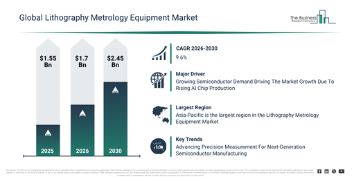
The lithography metrology equipment market has shown strong expansion in recent years. It is forecast to increase from $1.55 billion in 2025 to $1.7 billion in 2026, demonstrating a compound annual growth rate (CAGR) of 10.0%. Throughout the historical period, this growth can be attributed to factors like the escalating semiconductor manufacturing capacity, the rising demand for advanced semiconductor devices, the increasing adoption of smaller process nodes, the growing complexity of semiconductor fabrication, and the heightened necessity for improved manufacturing yield.
The lithography metrology equipment market is anticipated to experience substantial expansion over the upcoming years. Its valuation is projected to reach $2.45 billion by 2030, exhibiting a compound annual growth rate (CAGR) of 9.6%. This expansion during the projection period stems from several factors, including the rising need for 2 nanometer and smaller semiconductor manufacturing, the increased uptake of advanced packaging solutions, a surge in demand for high-resolution metrology setups, the expanding requirement for automated process management, and the wider implementation of multi-dimensional wafer inspection techniques. Key trends anticipated within the forecast timeframe encompass a heightened demand for precise lithography process evaluation, the growing incorporation of sophisticated overlay accuracy assessments, an escalating need for inspecting smaller feature dimensions, the expanded integration of real-time wafer measurement functionalities, and the increased implementation of highly sensitive defect detection platforms.
Get A Free Sample Report With In-Depth Market Insights:
Lithography Metrology Equipment Market Demand Drivers Opening New Revenue Streams
The increasing need for semiconductors is anticipated to drive expansion in the lithography metrology equipment market. Semiconductors are materials capable of conducting electricity under specific conditions, making them fundamental for producing integrated circuits (ICs), microchips, and numerous electronic devices. The surge in semiconductor demand stems from the widespread adoption of artificial intelligence (AI), which necessitates advanced chips for sophisticated computing, data processing, and machine learning applications across various sectors. This heightened semiconductor demand benefits lithography metrology equipment by escalating wafer production and increasing the requirement for exact critical dimension, overlay, and defect measurements, thereby ensuring greater manufacturing precision, output, and process oversight. For example, the Semiconductor Industry Association (SIA), a US-based trade association, reported in February 2026 that worldwide semiconductor sales rose from $630.5 billion in 2024 to $791.7 billion in 2025, marking a 25.6% increase. Consequently, the expanding semiconductor demand is a key factor driving the growth of the lithography metrology equipment market.
Lithography Metrology Equipment Market Breakdown By Product Type And Application
The lithography metrology equipment market covered in this report is segmented –
1) By Product Type: Critical Dimension Metrology Systems, Optical Critical Dimension Metrology Systems, Overlay Metrology Systems, Thin Film Metrology Systems, Scatterometry Metrology Systems, Mask (Reticle) Metrology Systems, Wafer Geometry Metrology Systems, Focus And Exposure Metrology Systems, Integrated Process Control Metrology Systems
2) By Node Technology: Above 10 Nanometers, 7–10 Nanometers, 5 Nanometers, 3 Nanometers, 2 Nanometers And Below
3) By Deployment: In Line Metrology, In Situ Metrology, Off Line Metrology
4) By Application: Logic Device Manufacturing, Memory Device Manufacturing, Advanced Packaging, Micro Electro Mechanical Systems Manufacturing, Compound Semiconductor Manufacturing
5) By End User Industry: Consumer Electronics, Telecommunications, Automotive, Healthcare, Aerospace And Defense
Subsegments:
1) By Critical Dimension Metrology Systems: Optical Critical Dimension Measurement, Electron Beam Critical Dimension Measurement, Hybrid Critical Dimension Measurement, Three Dimensional Critical Dimension Measurement
2) By Optical Critical Dimension Metrology Systems: Scatterometry Based Measurement, Reflectometry Based Measurement, Spectroscopic Ellipsometry Measurement, Multi Wavelength Optical Measurement
3) By Overlay Metrology Systems: Imaging Based Overlay Measurement, Diffraction Based Overlay Measurement, High Order Overlay Measurement, In Die Overlay Measurement
4) By Thin Film Metrology Systems: Film Thickness Measurement, Refractive Index Measurement, Optical Property Measurement, Layer Uniformity Measurement
5) By Scatterometry Metrology Systems: Angle Resolved Scatterometry, Spectroscopic Scatterometry, Imaging Scatterometry, Mueller Matrix Scatterometry
6) By Mask Metrology Systems: Mask Defect Inspection, Mask Critical Dimension Measurement, Mask Registration Measurement, Mask Surface Inspection
7) By Wafer Geometry Metrology Systems: Wafer Flatness Measurement, Wafer Bow Measurement, Wafer Warp Measurement, Edge Profile Measurement
8) By Focus And Exposure Metrology Systems: Focus Measurement, Exposure Dose Measurement, Focus Exposure Matrix Measurement, Process Window Measurement
9) By Integrated Process Control Metrology Systems: In Line Process Control, Real Time Process Monitoring, Closed Loop Process Control, Predictive Process Control
Lithography Metrology Equipment Market Trends Powering Strategic Industry Growth
Key companies within the lithography metrology equipment market are prioritizing the development of innovative solutions, such as high-precision electron beam metrology systems, to enhance measurement accuracy, optimize process control, and support the manufacturing of next-generation semiconductors. High-precision electron beam metrology systems are defined as advanced inspection and measurement devices that utilize focused electron beams to conduct exceptionally accurate dimensional and defect analyses of semiconductor wafers, enabling precise process management in sophisticated chip fabrication. For example, in December 2023, Hitachi High-Tech Corporation, a technology company from Japan, introduced the GT2000, a high-precision electron beam metrology system developed to deliver highly accurate measurement and inspection for advanced semiconductor devices utilized in the High-NA EUV (High Numerical Aperture Extreme Ultraviolet) lithography generation. This system offers advantages including high-resolution measurement accuracy, enhanced throughput for production environments, and improved support for both research and high-volume manufacturing. The objective of this launch is to assist semiconductor manufacturers in improving yield, accelerating advanced device development, and facilitating the industry’s move towards next-generation High-NA EUV lithography.
Lithography Metrology Equipment Market Competitive Overview And Top Companies
Major companies operating in the lithography metrology equipment market are ASML Holding N.V., Applied Materials Inc., KLA Corporation, Canon Inc., Nikon Corporation, Carl Zeiss AG, Hitachi High-Tech Corporation, Onto Innovation Inc., Nova Ltd., Lasertec Corporation, JEOL Ltd., Bruker Corporation, Veeco Instruments Inc., SUSS MicroTec SE, Camtek Ltd., Rigaku Holdings Corporation, HORIBA Ltd., Park Systems Corporation, Nearfield Instruments B.V., SCREEN Semiconductor Solutions Co. Ltd., Advantest Corporation
View The Full Lithography Metrology Equipment Market Report:
Lithography Metrology Equipment Market Leading Geography: Which Region Contributes The Most Revenue?
Asia-Pacific was the largest region in the lithography metrology equipment market in 2025. North America is expected to be the fastest-growing region in the forecast period. The regions covered in the lithography metrology equipment market report are Asia-Pacific, South East Asia, Western Europe, Eastern Europe, North America, South America, Middle East, Africa.
Reach Out To Our Team:
The Business Research Company: https://www.thebusinessresearchcompany.com/
Americas: +1 310-496-7795
Asia: +44 7882 955267 & +91 8897263534
Europe: +44 7882 955267
Email us at: marketing@tbrc.info
Follow us on:
LinkedIn: https://in.linkedin.com/company/the-business-research-company
YouTube: https://www.youtube.com/channel/UC24_fI0rV8cR5DxlCpgmyFQ
Global Market Model: https://www.thebusinessresearchcompany.com/global-market-model

Wasay has over a decade of experience in market research, data modelling, and analytics, with prior experience at GlobalData and Decision Tree Consulting Services. At The Business Research Company , he leads research operations across syndicated studies, customized consulting engagements, and the Global Market Model platform. His professional experience includes supporting organizations such as Boston Consulting Group, KPMG, and Ernst & Young. Wasay holds a degree in Electronics and Communications Engineering, postgraduate management qualifications from International Management Institute Belgium and Indian School of Business and Entrepreneurship, and completed the Integrated Program in Business Analytics from Indian Institute of Management Indore.