
Featuring market attractiveness scoring, total addressable market sizing, company benchmarking matrices, interactive Excel dashboards, deeper supply chain intelligence, emerging startup tracking, and granular product-level insights, The Business Research Company’s 2026 market reports are built to deliver research that is both more actionable and more strategically valuable.
Wafer Level Packaging Market Growth Potential: How Will Market Size Shift Through 2030?
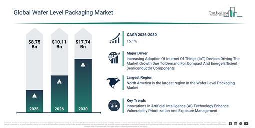
The wafer level packaging market has seen considerable growth in recent years. It is projected to increase from $8.75 billion in 2025 to $10.11 billion in 2026, demonstrating a compound annual growth rate (CAGR) of 15.5%. Historically, this growth was primarily driven by factors such as the increasing demand for more compact semiconductor packages, growing integration of semiconductor devices, the rising adoption of portable electronic devices, the increasing need for enhanced electrical performance, and the growing demand for reduced manufacturing costs.
The wafer level packaging market is anticipated to experience substantial growth over the next few years. It is projected to reach $17.74 billion in 2030, demonstrating a compound annual growth rate (CAGR) of 15.1%. This expansion during the forecast period is driven by factors such as the increasing demand for high-performance semiconductor devices, the rising adoption of advanced heterogeneous integration, the growing need for compact packages in automotive electronics, the expanding use of wafer level packaging in high-density computing applications, and the heightened requirement for improved thermal and signal performance. Key trends expected in this period include the increasing adoption of fan-out wafer level packaging, the growing utilization of hybrid bonding for advanced semiconductor packaging, the surging demand for three-dimensional wafer level integration, an intensified focus on miniaturized and high-density packaging structures, and the broader embrace of wafer-level packaging for heterogeneous integration.
Get A Free Sample Report With In-Depth Market Insights:
Wafer Level Packaging Market Growth Momentum: What Factors Are Shaping Demand?
The expanding use of internet of things (IoT) devices is anticipated to drive the future expansion of the wafer-level packaging market. These Internet of Things (IoT) devices are physical items equipped with sensors, software, and internet connectivity, enabling them to gather and share data. The proliferation of IoT devices stems from a rising need for automation, given that connected devices allow for real-time monitoring, data acquisition, and automated process control with minimal human input. IoT devices accelerate the adoption of wafer level packaging (WLP) by creating a demand for compact, efficient, reliable, and highly integrated semiconductor solutions crucial for future connected devices. As an example, the European Commission, a Belgium-based governing body, stated in July 2025 that the count of IoT-connected devices was approximately 40 billion in 2023 and is forecasted to climb to 49 billion by 2026, indicating an annual growth rate of 7%. Consequently, the expanding deployment of Internet of Things (IoT) devices is fueling the growth of the wafer-level packaging market.
Wafer Level Packaging Market Segment Trends And Revenue Contributors
The wafer level packaging market covered in this report is segmented –
1) By Packaging Type: Fan In Wafer Level Packaging, Fan Out Wafer Level Packaging, Wafer Level Chip Scale Packaging, Three Dimensional Wafer Level Packaging
2) By Interconnect Technology: Redistribution Layer Technology, Micro Bumping, Copper Pillar Bumping, Through Silicon Via, Hybrid Bonding
3) By Device Type: Logic Integrated Circuits, Memory Integrated Circuits, Radio Frequency And Analog Integrated Circuits, Sensors, Other Device Types
4) By Wafer Type: Silicon Based Wafer Level Packaging, Glass Based Wafer Level Packaging, Organic Substrates, Other Wafer Types
5) By End Use Application: Consumer Electronics, Automotive Electronics, Industrial Electronics, Internet Of Things Devices, Telecommunications Devices, Other End Use Applications
Subsegments:
1) By Fan In Wafer Level Packaging: Standard Fan In Wafer Level Packaging, High Density Fan In Wafer Level Packaging, Fine Pitch Fan In Wafer Level Packaging, Low Cost Fan In Wafer Level Packaging, Advanced Fan In Wafer Level Packaging
2) By Fan Out Wafer Level Packaging: Embedded Die Fan Out Packaging, High Density Fan Out Packaging, Large Panel Fan Out Packaging, Multi Die Fan Out Packaging, Advanced Fan Out Packaging
3) By Wafer Level Chip Scale Packaging: Single Die Wafer Level Chip Scale Packaging, Multi Die Wafer Level Chip Scale Packaging, Fine Pitch Wafer Level Chip Scale Packaging, Compact Wafer Level Chip Scale Packaging, Automotive Wafer Level Chip Scale Packaging
4) By Three Dimensional Wafer Level Packaging: Through Silicon Via Based Packaging, Stacked Die Packaging, Hybrid Bonding Packaging, Three Dimensional Integrated Circuit Packaging, Advanced Memory Packaging
Wafer Level Packaging Market Trends Redefining Industry Growth
Leading companies operating in the wafer level packaging market are concentrating on strategic investments to improve advanced semiconductor packaging capabilities. These strategic investments in wafer level packaging fuel market expansion by boosting manufacturing capacity, fostering the creation of next-generation semiconductor technologies, and enabling high-performance applications across sectors like automotive, aerospace, telecommunications, and defense. For instance, in May 2025, Foxconn Technology Group, a Taiwan-based electronics manufacturing company, announced a €250 million ($286 million) investment plan in Europe to establish advanced semiconductor packaging capabilities. This includes the region’s first fan-out wafer-level packaging (FOWLP) and outsourced semiconductor assembly and testing (OSAT) facility, formed through a joint venture with Thales and Radiall. The facility will harness advanced FOWLP technology to offer semiconductor packaging solutions for automotive, aerospace, 6G communications, and defense applications. This investment is projected to fortify regional semiconductor supply chains, enhance packaging efficiency, facilitate miniaturization and improved chip performance, and broaden the adoption of wafer-level packaging technologies in high-growth industries.
Wafer Level Packaging Market Competitive Landscape: Which Companies Lead The Industry?
Major companies operating in the wafer level packaging market are Taiwan Semiconductor Manufacturing Company Limited, Samsung Electronics Co Ltd, Intel Corporation, Broadcom Inc, Qualcomm Incorporated, Advanced Micro Devices Inc, SK Hynix Inc, ASE Technology Holding Co Ltd, Micron Technology Inc, MediaTek Inc, GlobalFoundries Inc, Infineon Technologies AG, STMicroelectronics NV, NXP Semiconductors NV, Amkor Technology Inc, Texas Instruments Incorporated, JCET Group Co Ltd, Powertech Technology Inc, Tongfu Microelectronics Co Ltd, Tianshui Huatian Technology Co Ltd, ChipMOS Technologies Inc, UTAC Holdings Ltd, Nepes Corporation, Chipbond Technology Corporation, Sony Group Corporation
View The Full Wafer Level Packaging Market Report:
Wafer Level Packaging Market Regional Breakdown: Where Is Demand Concentrated?
North America was the largest region in the wafer level packaging market in 2025. Asia-Pacific is expected to be the fastest-growing region in the forecast period. The regions covered in the wafer level packaging market report are Asia-Pacific, South East Asia, Western Europe, Eastern Europe, North America, South America, Middle East, Africa.
Reach Out To Our Team:
The Business Research Company: https://www.thebusinessresearchcompany.com/
Americas: +1 310-496-7795
Asia: +44 7882 955267 & +91 8897263534
Europe: +44 7882 955267
Email us at: marketing@tbrc.info
Follow us on:
LinkedIn: https://in.linkedin.com/company/the-business-research-company
YouTube: https://www.youtube.com/channel/UC24_fI0rV8cR5DxlCpgmyFQ
Global Market Model: https://www.thebusinessresearchcompany.com/global-market-model

Wasay has over a decade of experience in market research, data modelling, and analytics, with prior experience at GlobalData and Decision Tree Consulting Services. At The Business Research Company , he leads research operations across syndicated studies, customized consulting engagements, and the Global Market Model platform. His professional experience includes supporting organizations such as Boston Consulting Group, KPMG, and Ernst & Young. Wasay holds a degree in Electronics and Communications Engineering, postgraduate management qualifications from International Management Institute Belgium and Indian School of Business and Entrepreneurship, and completed the Integrated Program in Business Analytics from Indian Institute of Management Indore.