
Featuring market attractiveness scoring, total addressable market sizing, company benchmarking matrices, interactive Excel dashboards, deeper supply chain intelligence, emerging startup tracking, and granular product-level insights, The Business Research Company’s 2026 market reports are built to deliver research that is both more actionable and more strategically valuable.
Wide Bandgap Semiconductor Material And Devices Market Revenue Growth On Track For A 10.5% CAGR Through 2030
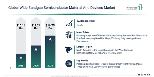
The wide bandgap semiconductor material and devices market has experienced significant expansion in recent years. It is projected to increase from $10.14 billion in 2025 to $11.24 billion in 2026, demonstrating a compound annual growth rate (CAGR) of 10.9%. The historical growth can be linked to factors such as the increasing demand for high-efficiency power electronics, the rising adoption of silicon carbide materials, the growing demand for high-temperature semiconductor devices, the increasing need for higher breakdown voltage, and the expansion of gallium nitride device manufacturing.
The wide bandgap semiconductor material and devices market size is anticipated to expand significantly over the next few years. It is projected to achieve a value of $16.75 billion by 2030, growing at a compound annual growth rate (CAGR) of 10.5%. This growth throughout the forecast period is driven by factors such as an escalating demand for next-generation power semiconductor devices, the increasing integration of wide bandgap devices in high-frequency applications, a rising need for high-power density electronics, the ongoing development of advanced gallium nitride and silicon carbide devices, and greater investment in wide bandgap semiconductor manufacturing capacity. Prominent trends for the forecast period include the growing adoption of gallium nitride semiconductor devices, enhanced deployment of silicon carbide power devices, an increasing requirement for high-temperature semiconductor operation, continued development of high-voltage wide bandgap devices, and broader integration of fast-switching semiconductor technologies.
Get A Free Sample Report With In-Depth Market Insights:
Wide Bandgap Semiconductor Material And Devices Market Growth Drivers: What’s Behind The Acceleration?
The increasing demand for electric vehicles is anticipated to boost the wide-bandgap semiconductor material and devices market moving forward. Electric vehicles are vehicles powered either fully or partially by electricity, utilizing electric motors and rechargeable batteries instead of relying entirely on internal combustion engines. The adoption of electric vehicles is expanding due to governmental incentives and more stringent emission regulations, making EVs more accessible and encouraging a shift towards cleaner transportation. The growing popularity of electric vehicles is fueling the need for wide-bandgap semiconductor materials and devices, as these facilitate greater power efficiency, quicker charging, and improved thermal management in EV drive systems and charging infrastructure. For instance, in January 2024, according to Kelley Blue Book, a US-based Cox Automotive company, 2023 saw a record 1.2 million car buyers in the United States choose electric vehicles, accounting for 7.6% of the entire U.S. vehicle market, an increase from 5.9% in 2022. Consequently, the rising demand for electric vehicles is propelling the expansion of the wide-bandgap semiconductor material and devices market.
Wide Bandgap Semiconductor Material And Devices Market Segment Outlook: Which Categories Are Growing Fastest?
The wide bandgap semiconductor material and devices market covered in this report is segmented –
1) By Type: Silicon Carbide, Gallium Nitride, Diamond Semiconductors, Aluminum Nitride, Gallium Oxide
2) By Voltage Range: Low Voltage, Medium Voltage, High Voltage, Extra High Voltage, Mixed Voltage Solutions
3) By Application: Power Electronics, Radio Frequency Devices, Optoelectronics, Electric Vehicles, Renewable Energy Systems
4) By End User: Automotive, Consumer Electronics, Industrial, Aerospace And Defense, Telecommunications
Subsegments:
1) By Silicon Carbide: Silicon Carbide Wafers, Silicon Carbide Substrates, Silicon Carbide Epitaxial Layers, Silicon Carbide Power Devices, Silicon Carbide Radio Frequency Devices
2) By Gallium Nitride: Gallium Nitride Wafers, Gallium Nitride Substrates, Gallium Nitride Epitaxial Layers, Gallium Nitride Power Devices, Gallium Nitride Radio Frequency Devices, Gallium Nitride Light Emitting Devices
3) By Diamond Semiconductors: Single Crystal Diamond Materials, Polycrystalline Diamond Materials, Diamond Power Devices, Diamond Radiation Detectors, Diamond Thermal Management Materials
4) By Aluminum Nitride: Aluminum Nitride Wafers, Aluminum Nitride Substrates, Aluminum Nitride Epitaxial Layers, Aluminum Nitride Power Devices, Aluminum Nitride Thermal Management Materials
5) By Gallium Oxide: Gallium Oxide Wafers, Gallium Oxide Substrates, Gallium Oxide Epitaxial Layers, Gallium Oxide Power Devices, Gallium Oxide Ultraviolet Photodetectors
Wide Bandgap Semiconductor Material And Devices Market Trends: What’s Defining The Industry’s Next Phase?
Leading companies operating in the wide-bandgap semiconductor material and devices market are concentrating on developing innovative solutions, such as enhanced epitaxial GaN-on-Si wafer scaling technology, to boost manufacturing efficiency, decrease production expenses, and facilitate the high-volume fabrication of next-generation power devices. This enhanced epitaxial GaN-on-Si wafer scaling technology involves sophisticated material growth and wafer fabrication techniques employed to deposit high-quality gallium nitride (GaN) layers onto silicon substrates at larger wafer sizes, enabling the scalable and cost-effective production of wide bandgap semiconductor devices. For instance, in September 2024, Infineon Technologies AG, a Germany-based semiconductor manufacturer, introduced its initial 300-mm power GaN wafer platform, designed to enable the high-volume manufacturing of GaN-based power semiconductor devices. This platform offers advantages such as improved production scalability, a lower cost per device, and higher energy efficiency. The launch aims to assist customers in achieving more efficient power electronics systems while supporting the industry’s transition toward scalable, cost-efficient wide-bandgap semiconductor manufacturing.
Wide Bandgap Semiconductor Material And Devices Market Leading Companies And Competitive Benchmarking
Major companies operating in the wide bandgap semiconductor material and devices market are Infineon Technologies AG, Mitsubishi Electric Corporation, STMicroelectronics NV, Texas Instruments Incorporated, Toshiba Electronic Devices & Storage Corporation, ON Semiconductor Corporation, NXP Semiconductors NV, Renesas Electronics Corporation, Sumitomo Electric Industries Ltd, Wolfspeed Inc, Resonac Holdings Corporation, Microchip Technology Incorporated, ROHM Co Ltd, Qorvo Inc, Coherent Corp, Fuji Electric Co Ltd, GlobalWafers Co Ltd, San’an Optoelectronics Co Ltd, Alpha & Omega Semiconductor Limited, MACOM Technology Solutions Holdings Inc, Soitec SA, Power Integrations Inc, SK siltron Co Ltd, Navitas Semiconductor Corporation, Innoscience (Suzhou) Technology Holding Co Ltd, Efficient Power Conversion Corporation, VisIC Technologies Ltd
View The Full Wide Bandgap Semiconductor Material And Devices Market Report:
Wide Bandgap Semiconductor Material And Devices Market Top Region By Revenue And Market Share
North America was the largest region in the wide bandgap semiconductor material and devices market in 2025. Asia-Pacific is expected to be the fastest-growing region in the forecast period. The regions covered in the wide bandgap semiconductor material and devices market report are Asia-Pacific, South East Asia, Western Europe, Eastern Europe, North America, South America, Middle East, Africa.
Reach Out To Our Team:
The Business Research Company: https://www.thebusinessresearchcompany.com/
Americas: +1 310-496-7795
Asia: +44 7882 955267 & +91 8897263534
Europe: +44 7882 955267
Email us at: marketing@tbrc.info
Follow us on:
LinkedIn: https://in.linkedin.com/company/the-business-research-company
YouTube: https://www.youtube.com/channel/UC24_fI0rV8cR5DxlCpgmyFQ
Global Market Model: https://www.thebusinessresearchcompany.com/global-market-model

Wasay has over a decade of experience in market research, data modelling, and analytics, with prior experience at GlobalData and Decision Tree Consulting Services. At The Business Research Company , he leads research operations across syndicated studies, customized consulting engagements, and the Global Market Model platform. His professional experience includes supporting organizations such as Boston Consulting Group, KPMG, and Ernst & Young. Wasay holds a degree in Electronics and Communications Engineering, postgraduate management qualifications from International Management Institute Belgium and Indian School of Business and Entrepreneurship, and completed the Integrated Program in Business Analytics from Indian Institute of Management Indore.