
Backed by market attractiveness analysis, total addressable market sizing, company benchmarking matrices, interactive Excel dashboards, wider supply chain intelligence, emerging startup coverage, and detailed product-level insights, The Business Research Company’s 2026 market reports are designed to offer research that is more actionable and strategically valuable than ever.
Semiconductor Equipment Packaging And Test Market Set To Climb From $39.83 Billion In 2026 To $48.92 Billion By 2030
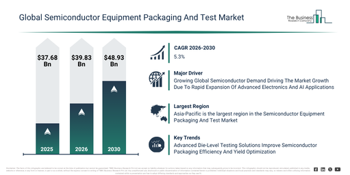
The semiconductor equipment packaging and test market has shown considerable growth in recent years. It is projected to expand from $37.68 billion in 2025 to $39.83 billion in 2026, exhibiting a compound annual growth rate (CAGR) of 5.7%. The historical increase can be ascribed to several factors, including the rising demand for semiconductors in consumer electronics, the ongoing expansion of semiconductor manufacturing facilities, the increasing integration of advanced integrated circuits, the heightened need for semiconductor quality assurance, and growing investments in semiconductor production infrastructure.
The semiconductor equipment packaging and test market is expected to witness substantial expansion in the upcoming years, projected to reach $48.93 billion by 2030, demonstrating a compound annual growth rate (CAGR) of 5.3%. This growth during the forecast period is primarily fueled by the increasing demand for advanced packaging solutions in AI chips, the rising adoption of automated semiconductor equipment, the ongoing development of next-generation testing technologies, the expansion of semiconductor fabrication capacity, and the growing need for high-performance computing and automotive semiconductors. Noteworthy trends over this period include the broadening use of advanced semiconductor packaging technologies for high-performance chips, the continued development of automated semiconductor testing and inspection equipment, the escalating demand for heterogeneous integration and chiplet packaging solutions, an increasing focus on miniaturized and high-density semiconductor packages, and the expanded deployment of advanced metrology systems for semiconductor quality control.
Get A Free Sample Report With In-Depth Market Insights:
Semiconductor Equipment Packaging And Test Market Growth Backed By Core Demand Fundamentals
The increasing worldwide need for semiconductors is anticipated to fuel expansion in the semiconductor equipment packaging and test market going forward. This global demand signifies the worldwide requirement for semiconductor chips and integrated circuits, which are essential in sectors like consumer electronics, automotive, telecommunications, and artificial intelligence. This heightened demand for semiconductors is primarily fueled by the rapid spread of artificial intelligence and technologies rich in data. Such applications necessitate more potent and specialized chips, compelling manufacturers to consistently boost their production capabilities. The rising demand for semiconductors in electronics, automotive, and AI uses elevates the need for sophisticated packaging and testing equipment. This is crucial for guaranteeing chip performance, reliability, and efficient high-volume production. An example illustrating this trend is that, as reported by the Semiconductor Industry Association, a US-based trade organization, in March 2026, global semiconductor sales reached $82.5 billion in January 2026. This represents a substantial 46.1% surge from the $56.5 billion recorded in January 2025. Consequently, the expanding global semiconductor demand is a key driver for the growth of the semiconductor equipment packaging and test market.
Semiconductor Equipment Packaging And Test Market Segments: Where Is Growth Concentrated?
The semiconductor equipment packaging and test market covered in this report is segmented –
1) By Equipment Type: Packaging Equipment, Test Equipment, Inspection And Metrology Equipment
2) By Automation Level: Semi Automated Equipment, Fully Automated Equipment
3) By Packaging Technology: Wire Bond Packaging, Flip Chip Packaging, Wafer Level Packaging, Fan Out Wafer Level Packaging, 2.5D Or 3D Packaging, Chiplet Packaging, Heterogeneous Integration Packaging
4) By Application: Logic Devices, Memory Devices, Analog Devices, Power Semiconductors, Radio Frequency Devices, Micro Electro Mechanical Systems And Sensors, Optoelectronic Devices
5) By End Use Industry: Consumer Electronics, Telecom, Computing And Networking, Industrial, Automotive Electronics, Healthcare, Information Technology And Telecommunication, Aerospace And Defence, Other End Use Industries
Subsegments:
1) By Packaging Equipment: Die Bonding Equipment, Wire Bonding Equipment, Flip Chip Bonding Equipment, Wafer Level Packaging Equipment, Encapsulation Equipment, Molding Equipment, Singulation Equipment, Marking Equipment, Ball Attach Equipment, Substrate Mounting Equipment
2) By Test Equipment: Wafer Testing Equipment, Final Testing Equipment, Burn In Testing Equipment, System Level Testing Equipment, Memory Testing Equipment, Logic Device Testing Equipment, Radio Frequency Testing Equipment, Mixed Signal Testing Equipment, Automated Handler Equipment, Probe Card Testing Equipment
3) By Inspection And Metrology Equipment: Optical Inspection Equipment, X Ray Inspection Equipment, Three Dimensional Inspection Equipment, Critical Dimension Measurement Equipment, Overlay Measurement Equipment, Surface Defect Inspection Equipment, Wafer Thickness Measurement Equipment, Package Inspection Equipment, Metrology Analysis Equipment, Process Control Inspection Equipment
#Semiconductor Equipment Packaging And Test Market Growth Trends: What’s Shaping The Future Outlook?
Leading firms within the semiconductor equipment packaging and test market are prioritizing the creation of sophisticated technologies, including integrated test cells. Their aim is to boost interconnect density, optimize signal performance, decrease power consumption, and facilitate the manufacturing of advanced semiconductor packages for high-performance computing and AI applications. These integrated test cells represent automated platforms that merge semiconductor testing apparatus, handling mechanisms, and software into a single, cohesive unit. This integration serves to simplify device validation, elevate testing efficiency, and increase overall production throughput. An example of this trend is Advantest Corporation, a Japanese semiconductor test equipment firm, which in December 2024 introduced the Advantest Known Good Die (KGD) Test Cell. This product was designed to refine the precision of known good die (KGD) testing, improve output rates, minimize the incorporation of faulty dies, and cater to advanced semiconductor packaging requirements. Noteworthy functionalities of this cell comprise proprietary probe card interface (PCI) technology, which safeguards probe cards and devices during high-voltage testing. It also features advanced die-level screening to stop defective dies from being introduced into power modules, along with integrated test-cell management to cut down on downtime and manufacturing losses.
Semiconductor Equipment Packaging And Test Market Key Participants And Competitive Landscape
Major companies operating in the semiconductor equipment packaging and test market are Advantest Corporation, ASMPT Limited, Teradyne Inc., DISCO Corporation, Kulicke & Soffa Industries Inc., BE Semiconductor Industries N.V., Onto Innovation Inc., Tokyo Seimitsu Co. Ltd., Hanmi Semiconductor Co. Ltd., EV Group, Cohu Inc., FormFactor Inc., SÜSS MicroTec SE, Hitachi High-Tech Corporation, Yamaha Motor Co. Ltd., Mycronic Group, Palomar Technologies Inc., Canon Machinery Inc., SET Corporation SA, TOWA Corporation
View The Full Semiconductor Equipment Packaging And Test Market Report:
Semiconductor Equipment Packaging And Test Market Regional Split: Which Areas Are Fueling Growth?
Asia-Pacific was the largest region in the semiconductor equipment packaging and test market in 2025. Asia-Pacific is expected to be the fastest-growing region in the forecast period. The regions covered in the semiconductor equipment packaging and test market report are Asia-Pacific, South East Asia, Western Europe, Eastern Europe, North America, South America, Middle East, Africa.
Reach Out To Our Team:
The Business Research Company: https://www.thebusinessresearchcompany.com/
Americas: +1 310-496-7795
Asia: +44 7882 955267 & +91 8897263534
Europe: +44 7882 955267
Email us at: marketing@tbrc.info
Follow us on:
LinkedIn: https://in.linkedin.com/company/the-business-research-company
YouTube: https://www.youtube.com/channel/UC24_fI0rV8cR5DxlCpgmyFQ
Global Market Model: https://www.thebusinessresearchcompany.com/global-market-model

Wasay has over a decade of experience in market research, data modelling, and analytics, with prior experience at GlobalData and Decision Tree Consulting Services. At The Business Research Company , he leads research operations across syndicated studies, customized consulting engagements, and the Global Market Model platform. His professional experience includes supporting organizations such as Boston Consulting Group, KPMG, and Ernst & Young. Wasay holds a degree in Electronics and Communications Engineering, postgraduate management qualifications from International Management Institute Belgium and Indian School of Business and Entrepreneurship, and completed the Integrated Program in Business Analytics from Indian Institute of Management Indore.