
Built to provide research that’s more actionable and strategically valuable, The Business Research Company’s 2026 market reports include market attractiveness analysis, total addressable market sizing, company benchmarking matrices, interactive Excel dashboards, broader supply chain intelligence, emerging startup tracking, and in-depth product insights.
Semiconductor Large Silicon Wafer Market CAGR Outlook And Future Development
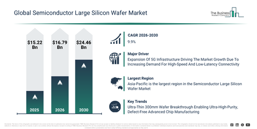
The semiconductor large silicon wafer market size has expanded rapidly in recent years. This market is projected to grow from $15.22 billion in 2025 to $16.79 billion in 2026, exhibiting a compound annual growth rate (CAGR) of 10.3%. The historic growth can be attributed to the increasing demand for semiconductor devices, the expansion of semiconductor fabrication facilities, the growing adoption of silicon based electronic components, rising production of consumer electronics devices, and increasing investments in semiconductor manufacturing infrastructure.
The semiconductor large silicon wafer market size is expected to experience significant expansion in the coming years. It is projected to reach $24.46 billion by 2030, demonstrating a compound annual growth rate (CAGR) of 9.9%. This growth throughout the forecast period is driven by increasing demand for high-performance computing applications, the rising adoption of advanced semiconductor nodes, the continuous expansion of semiconductor foundries, a growing need for high-efficiency wafer manufacturing processes, and the escalating production of automotive and power semiconductor devices. Noteworthy trends during this period include the wider embrace of larger diameter silicon wafers for advanced semiconductor manufacturing, an increasing demand for high-purity silicon substrates in next-generation integrated circuits, the ongoing development of ultra-large silicon wafers to enhance semiconductor production efficiency, a heightened focus on improved wafer quality and defect reduction technologies, and the worldwide proliferation of advanced wafer fabrication facilities.
Get A Free Sample Report With In-Depth Market Insights:
Semiconductor Large Silicon Wafer Market Demand Drivers Opening New Revenue Streams
The projected expansion of 5G infrastructure is anticipated to drive the advancement of the semiconductor large silicon wafer market in the future. This infrastructure encompasses a network of physical and digital elements, including small cells, base stations, antennas, fiber optic systems, and core network equipment, crucial for delivering fifth-generation wireless communication services. The surge in 5G infrastructure is fueled by a growing need for quicker data speeds, as contemporary applications like video streaming, cloud computing, and real-time communication demand considerably greater bandwidth and minimal latency for effective operation. The broadening of 5G infrastructure heightens the demand for sophisticated semiconductor devices, subsequently boosting the requirement for premium large silicon wafers. These wafers facilitate enhanced chip density, improved performance, and energy-efficient manufacturing processes essential for future communication systems. An illustration of this trend is seen in December 2023, when the Office of Communications (Ofcom), a UK-based government body, reported that the UK registered over 18,500 5G deployments spread across approximately 81,000 sites. This represents a substantial increase from approximately 12,000 deployments recorded in 2022. Consequently, the ongoing expansion of 5G infrastructure is a primary catalyst for the growth of the semiconductor large silicon wafer market.
Semiconductor Large Silicon Wafer Market Segment Landscape: Which Areas Lead Development?
The semiconductor large silicon wafer market covered in this report is segmented –
1) By Wafer Type: Polished Silicon Wafers, Epitaxial Silicon Wafers, Silicon On Insulator Wafers, Annealed Silicon Wafers
2) By Crystal Structure: Monocrystalline Silicon Wafers, Multicrystalline Silicon Wafers
3) By Wafer Size: 150 Millimeter, 200 Millimeter, 300 Millimeter, 450 Millimeter, Other Wafer Sizes
4) By Application: Logic Devices, Memory Devices, Power Semiconductor Devices, Analog Devices
5) By End User: Integrated Device Manufacturers, Foundries, Research Institutes And Universities
Subsegments:
1) By Polished Silicon Wafers: Prime Grade Polished Silicon Wafers, Double Side Polished Silicon Wafers, Single Side Polished Silicon Wafers, Test Grade Polished Silicon Wafers, Reclaimed Polished Silicon Wafers
2) By Epitaxial Silicon Wafers: Homoepitaxial Silicon Wafers, Heteroepitaxial Silicon Wafers, N Type Epitaxial Silicon Wafers, P Type Epitaxial Silicon Wafers
3) By Silicon On Insulator Wafers: Fully Depleted Silicon On Insulator Wafers, Partially Depleted Silicon On Insulator Wafers, Bonded Silicon On Insulator Wafers, Smart Cut Silicon On Insulator Wafers
4) By Annealed Silicon Wafers: Hydrogen Annealed Silicon Wafers, Argon Annealed Silicon Wafers, High Temperature Annealed Silicon Wafers, Rapid Thermal Annealed Silicon Wafers
Semiconductor Large Silicon Wafer Market Trends Powering Strategic Industry Growth
Leading companies within the large silicon wafer semiconductor market are concentrating on developing innovative solutions, including ultra-high-purity, defect-free 300 mm wafer fabrication technologies, to enhance chip yield, improve performance, and support advanced semiconductor scaling. Ultra-high-purity, defect-free 300 mm wafer fabrication technology describes advanced semiconductor manufacturing processes utilized to produce 300 mm silicon wafers with extremely low levels of chemical impurities and crystal defects, thereby enabling higher chip yields and improved performance in advanced integrated circuits. For instance, in October 2024, Infineon Technologies AG, a Germany-based semiconductor manufacturer, unveiled a breakthrough in ultra-thin silicon power wafer technology, showcasing 300-millimeter wafers with a thickness of just 20 micrometers. This advancement represents the thinnest silicon power wafer ever processed in high-scale manufacturing and is designed to significantly improve energy efficiency in power semiconductor applications. Additionally, this innovation allows for better material utilization and supports the company’s broader strategy of progressing silicon, silicon carbide, and gallium nitride technologies for next-generation decarbonized and digitalized systems.
Semiconductor Large Silicon Wafer Market Industry Leaders And Competitive Landscape
Major companies operating in the semiconductor large silicon wafer market are Shin-Etsu Chemical Co. Ltd., SUMCO Corporation, GlobalWafers Co. Ltd., Wacker Chemie AG, Siltronic AG, SK Siltron Co. Ltd., Soitec S.A., Entegris Inc., Wafer Works Corporation, Hangzhou Semiconductor Wafer Co. Ltd., Grinm Semiconductor Materials Co. Ltd., Shanghai Advanced Silicon Technology Co. Ltd., Okmetic Oy, Simgui Technology Co. Ltd., Phoenix Silicon International Corporation, Episil-Precision Inc., Zing Semiconductor Corporation, TotalFab Solutions
View The Full Semiconductor Large Silicon Wafer Market Report:
Semiconductor Large Silicon Wafer Market Global Footprint: Which Region Leads The Market?
Asia-Pacific was the largest region in the semiconductor large silicon wafer market in 2025. Asia-Pacific is expected to be the fastest-growing region in the forecast period. The regions covered in the semiconductor large silicon wafer market report are Asia-Pacific, South East Asia, Western Europe, Eastern Europe, North America, South America, Middle East, Africa.
Reach Out To Our Team:
The Business Research Company: https://www.thebusinessresearchcompany.com/
Americas: +1 310-496-7795
Asia: +44 7882 955267 & +91 8897263534
Europe: +44 7882 955267
Email us at: marketing@tbrc.info
Follow us on:
LinkedIn: https://in.linkedin.com/company/the-business-research-company
YouTube: https://www.youtube.com/channel/UC24_fI0rV8cR5DxlCpgmyFQ
Global Market Model: https://www.thebusinessresearchcompany.com/global-market-model

Wasay has over a decade of experience in market research, data modelling, and analytics, with prior experience at GlobalData and Decision Tree Consulting Services. At The Business Research Company , he leads research operations across syndicated studies, customized consulting engagements, and the Global Market Model platform. His professional experience includes supporting organizations such as Boston Consulting Group, KPMG, and Ernst & Young. Wasay holds a degree in Electronics and Communications Engineering, postgraduate management qualifications from International Management Institute Belgium and Indian School of Business and Entrepreneurship, and completed the Integrated Program in Business Analytics from Indian Institute of Management Indore.