Featuring market attractiveness scoring, total addressable market sizing, company benchmarking matrices, interactive Excel dashboards, deeper supply chain intelligence, emerging startup tracking, and granular product-level insights, The Business Research Company’s 2026 market reports are built to deliver research that is both more actionable and more strategically valuable.
3D Semiconductor Packaging Market CAGR Outlook And Future Development
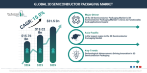
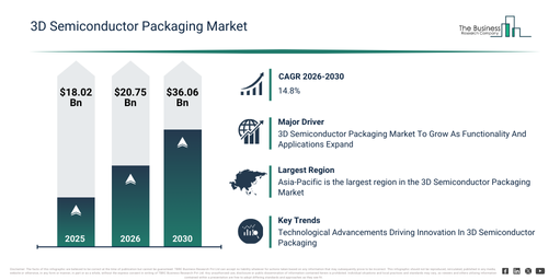
The 3D semiconductor packaging market size has seen rapid expansion over recent years. It is projected to increase from $18.02 billion in 2025 to $20.75 billion in 2026, demonstrating a compound annual growth rate (CAGR) of 15.2%. This historical growth can be attributed to several factors including the rise in conventional 2d packaging, the early integration of wire bonding, the expansion within computing and telecommunications, an increase in memory packaging applications, and the reliance on outsourced semiconductor packaging.
The 3D semiconductor packaging market is projected to experience substantial expansion over the upcoming years, with its size forecast to reach $36.06 billion by 2030, exhibiting a compound annual growth rate (CAGR) of 14.8%. This growth during the projection period can be attributed to the escalating demand for high-performance computing chips, the increasing embrace of heterogeneous integration, the proliferation of advanced system-in-package solutions, the evolution of low-power high-density architectures, and the growing application within automotive electronics. Key trends anticipated for the forecast timeframe encompass the emergence of AI-optimized chip stacking architectures, the broadening of high-density vertical integration platforms, the implementation of smart automated packaging systems, progress in IoT-enabled semiconductor manufacturing, and the incorporation of autonomous inspection and testing systems.
Get A Free Sample Report With In-Depth Market Insights:
3D Semiconductor Packaging Market Growth Factors: What’s Supporting Expansion?
The expansion of functions and application range for semiconductor or IC packages is anticipated to fuel the future growth of the 3D semiconductor packaging market. A semiconductor is defined as a solid material exhibiting electrical conductivities that fall between those of an insulator and a conductor. IC packaging serves as a prevalent technique for enhancing integration density and overall performance within a single package. As an illustration, data from July 2024, provided by the US-based government agency, the Bureau of Labor Statistics, indicated that in 2023, the cumulative trade value of exported semiconductors amounted to $65.9 billion, marking a 12.5% decrease relative to 2022. The six leading exporting states were responsible for 71.0% of this total trade value. Consequently, the expanded functionality and broader application scope of semiconductor or IC packages are propelling the 3D semiconductor packaging market.
3D Semiconductor Packaging Market Segment Outlook: Which Categories Are Growing Fastest?
The 3D semiconductor packaging market covered in this report is segmented –
1) By Type: 3D Through Silicon Via, 3D Package On Package, 3D Fan Out Based, 3D Wire Bonded
2) By Material: Organic Substrate, Bonding Wire, Leadframe, Encapsulation, Resins, Ceramic Packages, Die Attach Material, Other Materials
3) By Industry: Electronics, Industrial, Automotive And Transport, Healthcare, IT And Telecommunication Or Aerospace And Defense
Subsegments:
1) By 3D Through Silicon Via (TSV): Wafer-Level Packaging, System-In-Package (SiP), 3D Package On Package (PoP), Memory PoP, Logic PoP
2) By 3D Fan Out Based: Molded Fan-Out (MFO), Wafer Fan-Out (WFO)
3) By 3D Wire Bonded: Standard Wire Bonding, Advanced Wire Bonding Techniques
3D Semiconductor Packaging Market Industry Trends: What’s Reshaping Demand?
Leading corporations entering the semiconductor packaging market are adopting technological innovations like 3D stacking techniques for semiconductor packaging to lower production costs and customize products, thereby attracting clients. For instance, in January 2023, Canon, a US-based company, launched a semiconductor lithography i-line stepper system designed for 3D packaging technologies. This system features a resolution of 0.8 µm and is built to support current packaging trends. It offers cost-effective imaging solutions for both the front and back ends of the manufacturing line. Canon’s FPA-5520iV HR option for back-end i-line steppers reaches a resolution of 0.8 µm, addressing the evolving needs of the semiconductor industry. Additionally, Canon’s i-line steppers, such as the FPA-3030i5a and FPA-8000iW, can provide low-cost-of-ownership manufacturing for small substrates and advanced panel-level packaging (PLP) applications, respectively.
3D Semiconductor Packaging Market Leading Companies And Competitive Benchmarking
Major companies operating in the 3D semiconductor packaging market are Amkor Technology Inc., Advanced Semiconductor Engineering Inc., International Business Machines Corporation, Jiangsu Changjiang Electronics Technology Co. Ltd., Qualcomm Technologies Inc., Samsung Electronics Corporation Ltd., Siliconware Precision Industries Co. Ltd., STMicroelectronics NV, SÜSS MICROTEC SE, Taiwan Semiconductor Manufacturing Company Limited, 3M Company, Advanced Micro Devices Inc., Walton Advanced Engineering Inc., China Wafer Level CSP Co. Ltd., Chipbond Technology Corporation, Chipmos Technologies Inc., Lingsen Precision Industries Ltd., Micron Technology Inc., Powertech Technology Inc., Tokyo Electron Ltd., Toshiba Corporation, Unisem, United Microelectronics Corporation, United Test and Assembly Center Ltd., ON Semiconductor, Renesas Electronics Corporation, Skyworks Solutions Inc., Analog Devices, Inc., Broadcom Inc., Cypress Semiconductor Corporation, Maxim Integrated, Microchip Technology Inc., Texas Instruments Incorporated
View The Full 3D Semiconductor Packaging Market Report:
3D Semiconductor Packaging Market Top Region By Revenue And Market Share
Asia-Pacific was the largest region in the 3D semiconductor packaging market share in 2025. The regions covered in the 3D semiconductor packaging market report are Asia-Pacific, South East Asia, Western Europe, Eastern Europe, North America, South America, Middle East, Africa.
Reach Out To Our Team:
The Business Research Company: https://www.thebusinessresearchcompany.com/
Americas: +1 310-496-7795
Asia: +44 7882 955267 & +91 8897263534
Europe: +44 7882 955267
Email us at: marketing@tbrc.info
Follow us on:
LinkedIn: https://in.linkedin.com/company/the-business-research-company
YouTube: https://www.youtube.com/channel/UC24_fI0rV8cR5DxlCpgmyFQ
Global Market Model: https://www.thebusinessresearchcompany.com/global-market-model

Wasay has over a decade of experience in market research, data modelling, and analytics, with prior experience at GlobalData and Decision Tree Consulting Services. At The Business Research Company , he leads research operations across syndicated studies, customized consulting engagements, and the Global Market Model platform. His professional experience includes supporting organizations such as Boston Consulting Group, KPMG, and Ernst & Young. Wasay holds a degree in Electronics and Communications Engineering, postgraduate management qualifications from International Management Institute Belgium and Indian School of Business and Entrepreneurship, and completed the Integrated Program in Business Analytics from Indian Institute of Management Indore.