The Business Research Company’s 2026 market reports combine market attractiveness scoring, total addressable market sizing, company benchmarking matrices, interactive Excel dashboards, deeper supply chain intelligence, emerging startup tracking, and granular product-level insights to deliver research that is more actionable and strategically valuable.
What Is The Semiconductor Inspection Lens Market Growth Rate? A 9.3% CAGR Outlook Through 2030
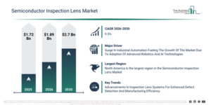
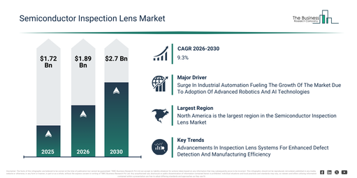
The semiconductor inspection lens market has experienced significant expansion recently. Its size is projected to increase from $1.72 billion in 2025 to $1.89 billion in 2026, demonstrating a compound annual growth rate (CAGR) of 9.6%. Historically, this market’s expansion was driven by factors such as the rising semiconductor manufacturing capacity, the early implementation of wafer inspection systems, a greater need for defect-free microelectronics, advancements in precision optical components, and an increase in research and development in microfabrication.
The semiconductor inspection lens market is projected to experience substantial expansion over the coming years. Its value is anticipated to reach $2.7 billion by 2030, demonstrating a compound annual growth rate (CAGR) of 9.3%. This anticipated growth stems from several factors, including increasing investments in advanced lithography technologies, the escalating requirement for nanoscale defect detection, the swift uptake of AI-driven inspection analytics, the proliferation of cloud-enabled inspection workflows, and the expansion of automated semiconductor production lines. Key trends during this period are expected to involve a heightened demand for ultra-high-resolution optical inspection, a greater emphasis on reducing optical aberrations for nanoscale imaging, the increasing implementation of modular lens architectures for enhanced inspection flexibility, a growing utilization of advanced coating technologies for precise imaging, and an accelerating move towards compact inspection lens systems for seamless integration into automated tools.
Access A Free Sample Of The Latest Semiconductor Inspection Lens Market Analysis:
Why Is The Semiconductor Inspection Lens Market Growing? The Key Demand Driver Explained
The future expansion of the semiconductor inspection lens market is anticipated due to increasing industrial automation. This automation involves employing technology and control systems to manage industrial operations and equipment with minimal human involvement. Its growth is driven by businesses implementing advanced robotics and AI to enhance manufacturing efficiency and lower running costs. Semiconductor inspection lenses support industrial automation by enabling precise, high-speed inspection of components, thereby guaranteeing quality and minimizing manual errors. For instance, in September 2025, the International Federation of Robotics, a Germany-based non-profit organization, projected global industrial robot installations to increase by 6% in 2025, reaching 575,000 units, and are expected to exceed 700,000 units by 2028. Consequently, the escalating industrial automation is a key driver for the growth of the semiconductor inspection lens market.
What Are The Main Segments Of The Semiconductor Inspection Lens Market?
The semiconductor inspection lens market covered in this report is segmented –
1) By Component: Hardware, Software, Services
2) By Type: Infrared Lenses, Ultraviolet Lenses, Visible Light Lenses
3) By Deployment Mode: On-Premises, Cloud-Based, Hybrid
4) By Application: Wafer Inspection, Package Inspection, Surface Inspection
5) By End-User Industry: Manufacturing, Research And Development, Academic Institutions, Government Agencies
Subsegments:
1) By Hardware: Lens Modules, Illumination Systems, Optomechanical Components, Sensors
2) By Software: Imaging Analysis Software, Defect Detection Software, Calibration Software, Process Optimization Software
3) By Services: Installation Services, Maintenance Services, Repair Services, Consulting Services
Semiconductor Inspection Lens Market Trend Analysis: Where Leading Companies Are Focusing
Key players in the semiconductor inspection lens market are prioritizing the development of innovative technological solutions, such as advanced semiconductor packaging inspection systems. These solutions are designed to boost defect detection accuracy, elevate yield rates, and streamline the entire manufacturing efficiency within semiconductor fabrication processes. Specifically, advanced semiconductor packaging inspection systems are sophisticated optical and imaging technologies employed to identify microscopic flaws and guarantee the quality and reliability of semiconductor packages during their production. For instance, in February 2025, TASMIT Inc., a Japan-based manufacturer of semiconductor inspection and measurement systems, launched a new large glass substrate inspection system under its INSPECTRA series. This groundbreaking system is the industry’s first to examine not only the front and back surfaces but also the internal structure of large glass substrates utilized in advanced semiconductor packaging, such as panel-level packaging (PLP). It effectively detects pattern defects, foreign particles, cracks, and other specific glass imperfections. Compatible with 650 mm square glass substrates, the system performs high-speed inspections in approximately 40 seconds per panel, thereby enabling 100% inspection to prevent defective products from reaching the market.
Which Companies Are Major Players In The Semiconductor Inspection Lens Market?
Major companies operating in the semiconductor inspection lens market are ASML Holding N.V., Applied Materials Inc., LG Innotek Co. Ltd., KLA Corporation, Synopsys Inc., Nikon Corporation, Hitachi High-Tech Corporation, Sunny Optical Technology Company Limited, SCREEN Holdings Co. Ltd., Carl Zeiss AG, Jenoptik AG, Leica Microsystems GmbH, Cohu Inc., Nova Ltd., Edmund Optics Inc., Dongguan Yutong Optical Technology Co.Ltd., Union Optech Co.Ltd., Moritex Corporation, Hong Kong VICO Technology Limited, Sill Optics GmbH & Co. KG,
Get The Complete Semiconductor Inspection Lens Market Analysis Here:
Which Region Held The Largest Share Of The Semiconductor Inspection Lens Market In 2025?
North America was the largest region in the semiconductor inspection lens market in 2025. The regions covered in the semiconductor inspection lens market report are Asia-Pacific, South East Asia, Western Europe, Eastern Europe, North America, South America, Middle East, Africa.
Reach Out To Our Team:
The Business Research Company: https://www.thebusinessresearchcompany.com/
Americas: +1 310-496-7795
Asia: +44 7882 955267 & +91 8897263534
Europe: +44 7882 955267
Email us at: marketing@tbrc.info
Follow us on:
LinkedIn: https://in.linkedin.com/company/the-business-research-company
YouTube: https://www.youtube.com/channel/UC24_fI0rV8cR5DxlCpgmyFQ
Global Market Model: https://www.thebusinessresearchcompany.com/global-market-model

Wasay has over a decade of experience in market research, data modelling, and analytics, with prior experience at GlobalData and Decision Tree Consulting Services. At The Business Research Company , he leads research operations across syndicated studies, customized consulting engagements, and the Global Market Model platform. His professional experience includes supporting organizations such as Boston Consulting Group, KPMG, and Ernst & Young. Wasay holds a degree in Electronics and Communications Engineering, postgraduate management qualifications from International Management Institute Belgium and Indian School of Business and Entrepreneurship, and completed the Integrated Program in Business Analytics from Indian Institute of Management Indore.