
Built to provide research that’s more actionable and strategically valuable, The Business Research Company’s 2026 market reports include market attractiveness analysis, total addressable market sizing, company benchmarking matrices, interactive Excel dashboards, broader supply chain intelligence, emerging startup tracking, and in-depth product insights.
Semiconductor Wafer Inspection Equipment Market Size And Revenue Outlook Through 2030
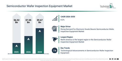
The semiconductor wafer inspection equipment market size has experienced substantial growth in recent years. This market is projected to expand from $6.52 billion in 2025 to $7.05 billion in 2026, at a compound annual growth rate (CAGR) of 8.1%. The historical expansion of this market can be attributed to the scaling of semiconductor manufacturing nodes, an increase in defect density within complex ICs, higher capital expenditure in wafer fabs, the demand for greater yield optimization, and the early adoption of optical inspection systems.
The semiconductor wafer inspection equipment market is anticipated to experience substantial expansion in the coming years, reaching a valuation of $9.67 billion by 2030, demonstrating a compound annual growth rate (CAGR) of 8.2%. This projected growth is driven by several factors, including the escalation in advanced logic and memory production, the global expansion of foundry capacity, the increasing intricacy of multilayer chip architectures, a heightened demand for real-time quality monitoring, and the incorporation of artificial intelligence and machine learning into inspection processes. Key trends expected during this period involve a greater embrace of AI-powered wafer inspection systems, the increasing implementation of inline and automated optical inspection instruments, a rising requirement for high-resolution defect detection at advanced manufacturing nodes, ongoing progress in electron beam and hybrid inspection technologies, and the broadening of real-time process control through integrated inspection solutions.
Get A Free Sample Report With In-Depth Market Insights:
Semiconductor Wafer Inspection Equipment Market Development Factors: What’s Supporting Demand?
The increasing requirement for electronic goods is anticipated to drive the expansion of the semiconductor wafer inspection equipment market. Electronic goods encompass products that employ electrical energy for operation, such as computers, smartphones, and various appliances. The surge in demand for these items is attributed to a growing reliance on technology for tasks like communication, entertainment, and everyday activities, propelled by continuous advancements in the electronics sector. Semiconductor wafer inspection equipment is essential for electronic goods to confirm the quality and reliability of semiconductor components by identifying and analyzing flaws during production. For instance, in February 2024, a report from USwitch, a UK-based online comparison and switching service provider, revealed that the UK recorded 71.8 million mobile connections at the beginning of 2022, exceeding its population by 4.2 million, which marked a 3.8% rise from the preceding year. It is projected that by 2025, with the UK population expected to reach 68.3 million, approximately 95% of people, or around 65 million, will be smartphone users. Consequently, the rising demand for electronic goods is fueling the growth of the semiconductor wafer inspection equipment market.
Semiconductor Wafer Inspection Equipment Market Segment Analysis And Revenue Potential
The semiconductor wafer inspection equipment market covered in this report is segmented –
1) By Type: Optical Inspection Systems, Electron Beam Inspection Systems, Other Types
2) By Application: Defect Detection, Metrology Or Measurement, Overlay Inspection, Wafer Edge Inspection, Film Thickness Measurement, Other Applications
3) By End-User: Foundries, Integrated Device Manufacturer (IDMs)
Subsegments:
1) By Optical Inspection Systems: 2D Optical Inspection Systems, 3D Optical Inspection Systems, Inline Optical Inspection Systems, Automated Optical Inspection (AOI) Systems
2) By Electron Beam Inspection Systems: Scanning Electron Microscope (SEM) Systems, Transmission Electron Microscope (TEM) Systems, E-Beam Metrology Systems
3) By Other Types: X-ray Inspection Systems, Atomic Force Microscopy (AFM) Systems, Laser-Based Inspection Systems, Ultrasound Inspection Systems
Semiconductor Wafer Inspection Equipment Market Transformation Trends: What Innovations Are Driving Change?
Leading companies in the semiconductor wafer inspection equipment market are innovating advanced solutions, such as non-patterned wafer surface inspection systems, to identify and analyze surface imperfections and irregularities early in manufacturing. A non-patterned wafer surface inspection system serves as a tool for detecting and scrutinizing surface flaws and inconsistencies on semiconductor wafers that lack existing patterns or circuits. As an illustration, in March 2024, Hitachi High-Tech Corporation, a Japan-based semiconductor wafer inspection equipment company, unveiled the LS9300AD. The LS9300AD represents a sophisticated system tailored for examining both the front and back of non-patterned wafer surfaces for particles and imperfections. It integrates traditional dark-field laser scattering detection with an innovative Differential Interference Contrast (DIC) inspection feature, enabling it to pinpoint unusual, shallow, and low-aspect microscopic defects. Employing the wafer edge grip technique and a rotating stage, the LS9300AD guarantees a thorough inspection of both wafer surfaces. This groundbreaking system from Hitachi High-Tech considerably lowers inspection expenditures and improves production yield for semiconductor wafer and device producers through its high-sensitivity and high-throughput identification of microscopic flaws.
Semiconductor Wafer Inspection Equipment Market Key Players Shaping Industry Direction
Major companies operating in the semiconductor wafer inspection equipment market are Applied Materials Inc., ASML Holding NV, Microtronic, Toray Industries Inc., Tokyo Electron Limited, KLA-Tencor, Hitachi High-Tec Corp., Nikon Corp., SCREEN Holdings Co. Ltd., Advantest Corporation, Bruker Corp., Teradyne Inc., Lasertec Corp., Cognex Corp., JEOL Ltd., Onto Innovation Inc., Veeco Instruments Inc., Cohu Inc., Nova Measuring Instruments Ltd., SUSS MicroTec Inc., Camtek Ltd., Nanometrics Inc., Ueno Seiki, Rudolph Technology & Associates, Carl Zeiss AG
View The Full Semiconductor Wafer Inspection Equipment Market Report:
Semiconductor Wafer Inspection Equipment Market Global Footprint: Which Region Leads The Market?
North America was the largest region in the semiconductor wafer inspection equipment market in 2025. Asia-Pacific is expected to be the fastest-growing region in the forecast period. The regions covered in the semiconductor wafer inspection equipment market report are Asia-Pacific, South East Asia, Western Europe, Eastern Europe, North America, South America, Middle East, Africa.
Reach Out To Our Team:
The Business Research Company: https://www.thebusinessresearchcompany.com/
Americas: +1 310-496-7795
Asia: +44 7882 955267 & +91 8897263534
Europe: +44 7882 955267
Email us at: marketing@tbrc.info
Follow us on:
LinkedIn: https://in.linkedin.com/company/the-business-research-company
YouTube: https://www.youtube.com/channel/UC24_fI0rV8cR5DxlCpgmyFQ
Global Market Model: https://www.thebusinessresearchcompany.com/global-market-model

Wasay has over a decade of experience in market research, data modelling, and analytics, with prior experience at GlobalData and Decision Tree Consulting Services. At The Business Research Company , he leads research operations across syndicated studies, customized consulting engagements, and the Global Market Model platform. His professional experience includes supporting organizations such as Boston Consulting Group, KPMG, and Ernst & Young. Wasay holds a degree in Electronics and Communications Engineering, postgraduate management qualifications from International Management Institute Belgium and Indian School of Business and Entrepreneurship, and completed the Integrated Program in Business Analytics from Indian Institute of Management Indore.