
Delivering more actionable and strategically valuable research, The Business Research Company’s 2026 market reports feature market attractiveness analysis, total addressable market evaluation, company benchmarking matrices, interactive Excel dashboards, expanded supply chain intelligence, emerging startup coverage, and detailed product insights.
Thin Wafer Processing And Dicing Equipment Market Value Analysis: What Growth Is Expected Over The Forecast Period?
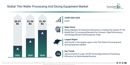
The thin wafer processing and dicing equipment market has demonstrated strong growth over recent years. Its valuation is set to rise from $0.97 billion in 2025 to $1.04 billion in 2026, achieving a compound annual growth rate (CAGR) of 7.9%. This historical expansion can be attributed to the escalating demand for miniaturized semiconductor devices, the wider adoption of advanced packaging technologies, the ongoing expansion of consumer electronics manufacturing, increasing investments in semiconductor fabrication facilities, and the growing requirement for high precision wafer processing equipment.
The thin wafer processing and dicing equipment market size is anticipated to experience robust growth over the coming years. It is projected to expand to $1.43 billion by 2030, achieving a compound annual growth rate (CAGR) of 8.2%. The expansion during the forecast period is attributable to increasing demand for AI and high-performance computing chips, the rising adoption of electric vehicles and power semiconductors, growing investment in next-generation semiconductor fabrication plants, the enlargement of MEMS and CMOS image sensor production, and ongoing innovation in automated laser and plasma dicing technologies. Significant trends for this period involve the increasing uptake of ultra-thin wafer processing technologies for compact semiconductor packaging, a heightened demand for precision laser dicing equipment to reduce wafer defects, the expanding utilization of automated wafer inspection systems for yield optimization, the ongoing development of low-damage wafer thinning technologies for advanced semiconductor devices, and the greater integration of high-accuracy wafer cleaning and polishing equipment in semiconductor manufacturing facilities.
Download A Free Sample Report For Comprehensive Market Insights:
https://www.thebusinessresearchcompany.com/sample_request?id=24345909&type=smp
#Thin Wafer Processing And Dicing Equipment Market Demand Drivers Creating New Revenue Opportunities
The increasing use of consumer electronics is anticipated to boost the growth of the thin wafer processing and dicing equipment market moving forward. These electronics encompass devices intended for everyday personal use, such as smartphones, televisions, laptops, and home entertainment systems. The surge in consumer electronics adoption is fueled by a rise in disposable income, which allows for greater expenditure on advanced devices and more frequent upgrades, alongside an increasing desire for innovative products packed with features. Thin wafer processing and dicing equipment are crucial for manufacturing ultra-thin, high-performance chips essential for compact consumer electronics, leading to better efficiency, reduced power usage, and improved device capabilities. For example, in May 2023, the Japan Electronics and Information Technology Industries Association, a Japan-based trade association, indicated that the total consumer electronic equipment production in Japan reached $209.16 million (¥32,099 million), a notable increase from $164.65 million (¥25,268 million) in May 2022. Consequently, the growing adoption of consumer electronics is a key driver for the thin wafer processing and dicing equipment market.
Thin Wafer Processing And Dicing Equipment Market Segment Breakdown: Which Categories Generate The Most Revenue?
The thin wafer processing and dicing equipment market covered in this report is segmented –
1) By Equipment Type: Dicing Equipment, Wafer Processing Equipment
2) By Wafer Thickness: 750 Micrometer, 120 Micrometer, 50 Micrometer
3) By Wafer Size: 200 Millimeter, 300 Millimeter, Other Wafer Sizes
4) By Application: Memory Devices, Logic Devices, Micro-Electro-Mechanical Systems, Power Devices, Radio-Frequency Identification, Complementary Metal-Oxide-Semiconductor Image Sensors, Other Applications
5) By End-User: Semiconductor Manufacturers, Foundries, Other End Users
Subsegments:
1) By Dicing Equipment: Blade Dicing Equipment, Laser Dicing Equipment, Plasma Dicing Equipment, Stealth Dicing Equipment, Automatic Wafer Dicing Equipment
2) By Wafer Processing Equipment: Wafer Grinding Equipment, Wafer Polishing Equipment, Wafer Thinning Equipment, Wafer Cleaning Equipment, Wafer Inspection Equipment
Thin Wafer Processing And Dicing Equipment Market Trends Driving Strategic Industry Expansion
Leading companies in the thin wafer processing and dicing equipment market are concentrating on developing advanced solutions, such as extreme laser lift-off systems, with the goal of improving precision, reducing material damage, and enhancing processing efficiency for wafer-bonded devices. Laser lift-off is a technology employed to separate thin semiconductor layers from carrier substrates using high-energy laser pulses, which enables the fabrication of ultra-thin and high-performance devices. As an illustration, in December 2024, Tokyo Electron, a Japan-based semiconductor equipment manufacturer, unveiled Ulucus LX, an extreme laser lift-off system tailored for 300 mm wafer-bonded devices. This system allows for high-throughput and damage-free separation of bonded wafers, thereby supporting advanced semiconductor packaging and boosting overall device performance and manufacturing efficiency.
Thin Wafer Processing And Dicing Equipment Market Key Players And Strategic Industry Positioning
Major companies operating in the thin wafer processing and dicing equipment market are Panasonic Connect Co. Ltd, Lam Research Corporation, KLA Corporation, Han’s Laser Technology Industry Group Co. Ltd, DISCO Corporation, ASMPT Limited, Kulicke and Soffa Industries Inc, Veeco Instruments Inc, EV Group GmbH, SUSS MicroTec SE, MTI Corporation, Hanmi Semiconductor Co. Ltd, Plasma-Therm LLC, Tokyo Seimitsu Co. Ltd, AXUS Technology Inc, Yamamoto Manufacturing Co. Ltd, NeonTech Co. Ltd, Synova SA, Citizen Chiba Precision Co. Ltd, Dynatex International Inc, Suzhou Delphi Laser Co. Ltd, Loadpoint Limited
Access The Complete Thin Wafer Processing And Dicing Equipment Market Report:
#Thin Wafer Processing And Dicing Equipment Market Largest Region: Which Geography Holds The Highest Market Share?
Asia-Pacific was the largest region in the thin wafer processing and dicing equipment market in 2025. Asia-Pacific is expected to be the fastest-growing region in the forecast period. The regions covered in the thin wafer processing and dicing equipment market report are Asia-Pacific, South East Asia, Western Europe, Eastern Europe, North America, South America, Middle East and Africa.
Get in touch with us:
The Business Research Company: https://www.thebusinessresearchcompany.com/
Americas: +1 310-496-7795
Asia: +44 7882 955267 & +91 8897263534
Europe: +44 7882 955267
Email us at: marketing@tbrc.info
Follow us on:
LinkedIn: https://in.linkedin.com/company/the-business-research-company
YouTube: https://www.youtube.com/channel/UC24_fI0rV8cR5DxlCpgmyFQ
Global Market Model: https://www.thebusinessresearchcompany.com/global-market-model

Wasay has over a decade of experience in market research, data modelling, and analytics, with prior experience at GlobalData and Decision Tree Consulting Services. At The Business Research Company , he leads research operations across syndicated studies, customized consulting engagements, and the Global Market Model platform. His professional experience includes supporting organizations such as Boston Consulting Group, KPMG, and Ernst & Young. Wasay holds a degree in Electronics and Communications Engineering, postgraduate management qualifications from International Management Institute Belgium and Indian School of Business and Entrepreneurship, and completed the Integrated Program in Business Analytics from Indian Institute of Management Indore.