
Through market attractiveness analysis, total addressable market evaluation, company benchmarking matrices, interactive Excel dashboards, expanded supply chain intelligence, emerging startup coverage, and detailed product insights, The Business Research Company’s 2026 market reports provide more actionable and strategically valuable research.
Wafer Foundry Service Market Forecast: What Market Value Is Expected By 2030?
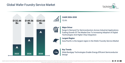
The wafer foundry service market has experienced rapid expansion in recent years. This market is projected to increase from $132.44 billion in 2025 to $149.56 billion in 2026, showing a compound annual growth rate (CAGR) of 12.9%. The historical growth of the market can be linked to several factors, including heightened demand for advanced process nodes, the increasing adoption of the fabless semiconductor business model, a rise in consumer electronics production, the broadening scope of automotive and EV semiconductor applications, and the ongoing rollout of 4G and 5G communication infrastructure.
The wafer foundry service market is projected for substantial expansion over the upcoming years. This market is anticipated to reach $240.60 billion by 2030, exhibiting a compound annual growth rate (CAGR) of 12.6%. Factors contributing to this projected growth include the escalating demand for AI and HPC workloads, the growing uptake of automotive-grade wafers, the expanding application of specialized materials (SiC, GaN, SOI), the proliferation of regional initiatives for semiconductor self-sufficiency, and the heightened integration of backend value-added processes. Key trends during this period are expected to encompass an escalating need for advanced process nodes, the broader embrace of the fabless semiconductor business model, increased manufacturing of consumer electronics, the broadening scope of semiconductor applications in automotive and EV, and the continued deployment of 4G and 5G communication infrastructure.
Download A Free Sample Report For Comprehensive Market Insights:
#Wafer Foundry Service Market Growth Factors: Which Forces Are Supporting Market Expansion?
The increasing requirement for semiconductors in industrial applications is projected to fuel the expansion of the wafer foundry service market moving forward. This refers to the rising need for semiconductor chips that enable functionality across a wide array of modern devices, including personal gadgets, vehicles, and industrial automation systems. The growth in demand for semiconductors across industrial applications is occurring as manufacturers and consumers increasingly adopt digital technologies, embedding more chips per product to improve both performance and connectivity. Wafer foundry services support semiconductors in industrial applications by providing the essential fabrication capacity and advanced process technologies that design-focused companies depend on to manufacture integrated circuits efficiently and with high quality. For instance, in December 2025, the Semiconductor Industry Association, a US-based nonprofit trade association, reported that global semiconductor sales reached $72.7 billion in October 2025, representing a 4.7% increase from $69.5 billion in September 2025 and a 27.2% rise compared to the $57.2 billion observed in October 2024. Therefore, the expanding demand for semiconductors in industrial applications is a primary driver behind the growth of the wafer foundry service market.
Wafer Foundry Service Market Segment Landscape: Which Areas Lead Market Development?
The wafer foundry service market covered in this report is segmented –
1) By Cutting-Edge: Cutting-Edge (3/5/7nm), 10/14/16/20/28nm, 40/45/65nm, 90nm, 11/0.13µm, 15/0.18µm, >0.25µm
2) By Wafer Size: 150 Mm, 200 Mm, 300 Mm, 450 Mm
3) By Material Or Substrate Type: Silicon (SI), Silicon-On-Insulator (SoI), Silicon Carbide (SiC), Gallium Nitride (GAN), Other Compound Semiconductors
4) By Wafer Or Technology Platform: CMOS Logic Foundry Services, Analog And Mixed-Signal Foundry Services, RF And Mmwave Foundry Services, Power And Wide-Bandgap (SiC, GaN) Foundry Services, MEMS And Sensor Foundry Services, Specialty Or Embedded
5) By Application: Consumer Electronics, Computing And Data Center (AI, HPC, Cloud), Automotive And EV, Industrial And Power Electronics, Communications Or 5G Or RF, Healthcare And IoT Or Wearables, Aerospace And Defense
Subsegments:
1) By Cutting-Edge (3/5/7nm): High Performance Logic Chips, Advanced Graphics Processors, Artificial Intelligence Processors, Mobile System-on-Chips, Cloud Data Center Chips
2) By 10/14/16/20/28nm: Consumer Electronics Chips, Automotive Microcontrollers, Networking Chips, Industrial Control ICs, Communication Processors
3) By 40/45/65nm: Analog Integrated Circuits, Power Management ICs, Sensor Interface Chips, Display Driver ICs, Microcontrollers
4) By 90nm: Memory Chips, Mixed Signal ICs, Audio And Video Processors, Low Power Microcontrollers, Standard Logic ICs
5) By 11/0.13µm: Embedded Control Chips, Automotive Electronics, Industrial Power ICs, Consumer Interface Chips, Mixed Signal Devices
6) By 15/0.18µm: High Voltage ICs, Display Driver Chips, Analog Power ICs, Automotive Safety ICs, Communication Chips
7) By >0.25µm: Smart Card Chips, Security ICs, Low Frequency Communication Chips, Power Devices, Legacy Industrial ICs
Wafer Foundry Service Market Industry Trends: What Changes Are Reshaping Demand?
Key companies operating in the wafer foundry service market are prioritizing technological advancements, such as GaN-on-Si foundry services designed for depletion-mode devices. This strategic focus aims to accelerate prototyping, support high-volume production, and expand access to advanced wide-bandgap semiconductor technologies. GaN-on-Si foundry services integrate deep expertise in high-voltage GaN processes with capabilities for multi-project wafer (MPW) and scalable manufacturing, which collectively enable more rapid development cycles and wider adoption of energy-efficient, high-performance devices. As an illustration, in September 2025, X-FAB Silicon Foundries SE, a Belgium-based specialist in semiconductor foundries, launched GaN-on-Si foundry services specifically for depletion-mode (dMode) devices, utilizing its XG035 technology platform. This process is hosted at X-Fab’s automotive-qualified 8-inch fabrication facility in Dresden, which is equipped with specialized tools designed for processing thick GaN-on-Si wafers. The service additionally offers open-access multi-project wafer (MPW) options, prototyping, and volume production solutions, facilitating faster and more cost-effective development cycles for customers. It also enhances X-Fab’s current portfolio of wide-bandgap technologies, which includes silicon carbide (SiC), and is optimized for analog-CMOS integration, thereby opening new opportunities for mixed-signal and power-efficient applications.
Wafer Foundry Service Market Industry Leaders And Market Competition
Major companies operating in the wafer foundry service market are Samsung Electronics Co. Ltd., Taiwan Semiconductor Manufacturing Company Limited, Intel Corporation, Texas Instruments Incorporated, STMicroelectronics N.V., Microchip Technology Incorporated, Semiconductor Manufacturing International Corporation, GlobalFoundries Inc., United Microelectronics Corporation, ams-OSRAM AG, Hua Hong Semiconductor Ltd., Sanan Optoelectronics Co. Ltd., Tower Semiconductor Ltd., Powerchip Semiconductor Manufacturing Corporation (PSMC), Vanguard International Semiconductor Corporation (VIS), Fujitsu Semiconductor Ltd., X-FAB Silicon Foundries SE, DB HiTek Co. Ltd., WIN Semiconductors, SilTerra Malaysia Sdn. Bhd, Nexchip Semiconductor Corporation
Access The Complete Wafer Foundry Service Market Report:
Wafer Foundry Service Market Leading Geography: Which Region Generates The Most Revenue?
Asia-Pacific was the largest region in the wafer foundry service market in 2025. North America is expected to be the fastest-growing region in the forecast period. The regions covered in the wafer foundry service market report are Asia-Pacific, South East Asia, Western Europe, Eastern Europe, North America, South America, Middle East, Africa.
Get in touch with us:
The Business Research Company: https://www.thebusinessresearchcompany.com/
Americas: +1 310-496-7795
Asia: +44 7882 955267 & +91 8897263534
Europe: +44 7882 955267
Email us at: marketing@tbrc.info
Follow us on:
LinkedIn: https://in.linkedin.com/company/the-business-research-company
YouTube: https://www.youtube.com/channel/UC24_fI0rV8cR5DxlCpgmyFQ
Global Market Model: https://www.thebusinessresearchcompany.com/global-market-model

Wasay has over a decade of experience in market research, data modelling, and analytics, with prior experience at GlobalData and Decision Tree Consulting Services. At The Business Research Company , he leads research operations across syndicated studies, customized consulting engagements, and the Global Market Model platform. His professional experience includes supporting organizations such as Boston Consulting Group, KPMG, and Ernst & Young. Wasay holds a degree in Electronics and Communications Engineering, postgraduate management qualifications from International Management Institute Belgium and Indian School of Business and Entrepreneurship, and completed the Integrated Program in Business Analytics from Indian Institute of Management Indore.