
Delivering more actionable and strategically valuable research, The Business Research Company’s 2026 market reports feature market attractiveness analysis, total addressable market evaluation, company benchmarking matrices, interactive Excel dashboards, expanded supply chain intelligence, emerging startup coverage, and detailed product insights.
Ceramic Substrates In Electronic Packaging Market Value Analysis: What Growth Is Expected Over The Forecast Period?
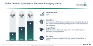
The ceramic substrates in electronic packaging market has experienced robust growth in recent years. It is forecast to increase from $5.58 billion in 2025 to $5.92 billion in 2026, exhibiting a compound annual growth rate (CAGR) of 6.0%. The historical expansion of this market can be attributed to the growth of power electronics manufacturing, the development of telecommunications infrastructure, the integration of ceramic substrates into aerospace systems, the increasing demand for reliable electronic packaging, and the availability of advanced ceramic materials.
The ceramic substrates in electronic packaging market is anticipated to experience substantial growth in the upcoming years, with its size projected to reach $7.48 billion by 2030, achieving a compound annual growth rate (CAGR) of 6.0%. This expansion during the forecast period is attributed to several factors including the increasing deployment of electric vehicles, the growth of high-frequency electronics, rising investments in advanced semiconductor packaging, increasing demand for thermal management solutions, and the expansion of automotive electronics. Significant trends expected during this period include the escalating use in high-power electronic applications, a rising demand for high thermal conductivity substrates, growing adoption in electric vehicles, the expansion of advanced packaging technologies, and an enhanced focus on miniaturization.
Download A Free Sample Report For Comprehensive Market Insights:
Ceramic Substrates In Electronic Packaging Market Development Factors: Which Trends Are Supporting Demand?
The increasing need for miniaturized electronics is anticipated to boost the expansion of the ceramic substrates in electronic packaging market. Miniaturized electronics refer to more compact electronic devices and components that perform the same functions as larger ones but occupy less space, often enhancing efficiency and performance. This rising demand for miniaturized electronics is fueled by the requirement for convenient, more powerful devices such as smartphones, wearables, and IoT products. As technology progresses, both consumers and businesses desire products that are efficient and portable while still delivering high performance. Ceramic substrates find application in miniaturized electronics to support and connect smaller components within a confined area. They contribute to improving the durability and efficiency of these devices, making them suitable for high-performance, small-scale electronics. For instance, in November 2025, a report published by the Semiconductor Industry Association, a US-based trade association, stated Semiconductor Sales Surge, Q3 2025 Hits $208.4 Billion, Up 15.8% from Q2 and 7.0% Monthly Growth in September. Thus, the growing demand for miniaturized electronics is a significant driver for the growth of ceramic substrates in electronic packaging market.
Ceramic Substrates In Electronic Packaging Market Segment Analysis: What Are The Major Market Categories?
The ceramic substrates in electronic packaging market covered in this report is segmented –
1) By Type: Alumina(Al2O3), Aluminum Nitride(AlN), Beryllium Oxide(BeO), Silicon Nitride (Si3N4)
2) By Application: Power Electronics, Electronic Packaging, Hybrid Microelectronics, Multi-Chip Modules
3) By End-User: Automotive, Telecommunications, Consumer Electronics, Aerospace And Defense, Other End Users
Subsegments:
1) By Alumina (Al₂O₃): High-Purity Alumina Substrates, Standard Alumina Substrates, Thick-Film Alumina Substrates, Thin-Film Alumina Substrates
2) By Aluminum Nitride (AlN): High Thermal Conductivity AlN Substrates, Low-Temperature Co-Fired AlN Substrates, Thin-Film AlN Substrates
3) By Beryllium Oxide (BeO): High Thermal Conductivity BeO Substrates, Microwave and RF BeO Substrates, High-Purity BeO Substrates
4) By Silicon Nitride (Si₃N₄): High-Strength Si₃N₄ Substrates, Automotive-Grade Si₃N₄ Substrates, Thin-Film Si₃N₄ Substrates
Ceramic Substrates In Electronic Packaging Market Trends Reshaping Industry Growth
Companies operating within the ceramic substrates in electronic packaging market are increasingly making strategic investments, such as establishing advanced manufacturing plants, to boost their production capabilities, satisfy escalating demand, and enhance the efficiency of their supply chains. An advanced manufacturing plant is a sophisticated factory that leverages modern technologies like automation, robotics, and artificial intelligence to produce goods with greater efficiency and precision. For example, in November 2024, Heraeus Electronics, a Germany-based firm known for materials used in assembling and packaging electronic devices, opened a state-of-the-art facility in the Changshu New & Hi-tech Industrial Development Zone (CNZ), Jiangsu Province, China. This new site is dedicated to the manufacturing of high-performance semiconductor metal ceramic substrates, which encompass Active Metal Brazed (AMB) substrates. These sophisticated products cater to vital industries such as electric vehicles, wind energy, and photovoltaics, aligning with China’s strategic objectives of achieving carbon peak and carbon neutrality.
Ceramic Substrates In Electronic Packaging Market Leading Companies Driving Competitive Growth
Major companies operating in the ceramic substrates in electronic packaging market are Compagnie de Saint-Gobain, Heraeus Holding GmbH, Toshiba Corporation, TDK Corporation, Kyocera Corporation, Murata Manufacturing Co. Ltd., NGK Spark Plug Co. Ltd., Vishay Intertechnology Inc., Schott AG, CoorsTek Inc., Morgan Advanced Materials plc, Rogers Corporation, Chaozhou Three-Circle (Group) Co. Ltd., CeramTec GmbH, Yokowo Co. Ltd., Tong Hsing Electronic Industries Ltd., Maruwa Co. Ltd., Nippon Carbide Industries Co. Inc., KOA Corporation, Ferro Corporation.
Access The Complete Ceramic Substrates In Electronic Packaging Market Report:
Ceramic Substrates In Electronic Packaging Market Global Footprint: Which Region Holds Market Leadership?
North America was the largest region in the ceramic substrates in electronic packaging market in 2025. Asia-Pacific is expected to be the fastest-growing region in the forecast period. The regions covered in the ceramic substrates in electronic packaging market report are Asia-Pacific, South East Asia, Western Europe, Eastern Europe, North America, South America, Middle East, Africa.
Get in touch with us:
The Business Research Company: https://www.thebusinessresearchcompany.com/
Americas: +1 310-496-7795
Asia: +44 7882 955267 & +91 8897263534
Europe: +44 7882 955267
Email us at: marketing@tbrc.info
Follow us on:
LinkedIn: https://in.linkedin.com/company/the-business-research-company
YouTube: https://www.youtube.com/channel/UC24_fI0rV8cR5DxlCpgmyFQ
Global Market Model: https://www.thebusinessresearchcompany.com/global-market-model

Wasay has over a decade of experience in market research, data modelling, and analytics, with prior experience at GlobalData and Decision Tree Consulting Services. At The Business Research Company , he leads research operations across syndicated studies, customized consulting engagements, and the Global Market Model platform. His professional experience includes supporting organizations such as Boston Consulting Group, KPMG, and Ernst & Young. Wasay holds a degree in Electronics and Communications Engineering, postgraduate management qualifications from International Management Institute Belgium and Indian School of Business and Entrepreneurship, and completed the Integrated Program in Business Analytics from Indian Institute of Management Indore.